Part Number: ALM2403-Q1
Currently, I intend to use the ALM2403-Q1 as the amplifier for the AU6805.
The AU6805 outputs a waveform, not PWM.
Is the ALM2403-Q1 usable without any problems?
If there are no issues, I would like to see an example circuit.
This thread has been locked.
If you have a related question, please click the "Ask a related question" button in the top right corner. The newly created question will be automatically linked to this question.
Part Number: ALM2403-Q1
Currently, I intend to use the ALM2403-Q1 as the amplifier for the AU6805.
The AU6805 outputs a waveform, not PWM.
Is the ALM2403-Q1 usable without any problems?
If there are no issues, I would like to see an example circuit.
Hello Takaya-san,
Welcome to the E2E Forum.
ALM2403-Q1 is an excellent choice for this application, and the output of an analog waveform actually makes the circuit easier to implement.
To start, we need to confirm a few parameters:
1. What is the desired output excitation amplitude desired on the resolver
2. What is the impedance of the resolver
3. What are the available supply rails to the ALM amplifier
We can still create a simplified version of the schematic while we wait on clarification regarding the fine details.
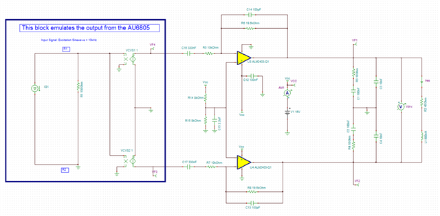
Here is a simplified version of the ALM schematic which should work for your purposes:

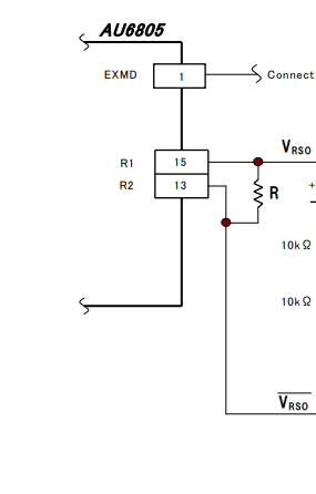
Note, my 150 Ohm resistors are before my ground splitter circuit, but in reality, this R1 would be included between the input terminals on your PCB like this:

Here is the output from this block:

I am including a simulation file here for you to adjust as desired.
Once I hear back regarding you applications details, we can update all components to be best fit to your system.
Please let me know if you have any questions.
Best,
Jacob
Hi Takaya-san,
Here is the updated schematic:

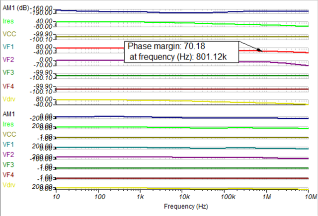
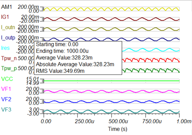
Good transient performance:

Stable phase margin (no unexpected oscillations due to control loop instability)

RMS current draw per channel is ~350mW, meaning total chip power consumption will be ~700mW

If we look at the datasheet, this gives us an expected junction temperature increase of about TJ= Ta + .7W * 22.6W/C = Ta + ~16C

Please let me know if you have any questions.
Best,
Jacob
Thank you, Jacob.
I have a few questions.
1. Is a capacitor not needed for VCC on U4?
2. Is it okay to connect 15V directly to the V+ pin of the IC's 11th pin?
That's all.
Hi Takaya-san,
1.You are correct, ideally this connection at U4 should have a decoupling capacitor as well.
2. Yes, you can connect 15V directly to pin 11, so long as you also connect 15V to pins 12 and 10.
Most designs tend to use a decoupling capacitor for each pin (like below), but you could also route this as one large copper trace connecting all pins 10-12 together

Please let me know if you have any questions.
Best,
Jacob
Thank you, Jacob.
I have some additional questions.
1. What input current does the "Signal input current" in the absolute maximum ratings for the ALM2403-Q1 refer to?
2. If it's IN1/2, the AU6805 is outputting 20mArms, but is the ±10mA rating acceptable?
That's all.
Hi Takaya-san,
Input current refers to the maximum current that can flow into INx+ or INx-. Note, this current is typically just the CMOS gate current, so think on the order of single digit pA.
What will however cause large conduction would be ESD or over-voltage events.
AU6805 will use the 20mA to generate voltage across the burden resistor, but this current flow will not go through the input terminals of the op amp so long as the device has VCC connected to V+.
Please let me know if you have any questions, I can build up a simulation file if it does not make sense.
Thanks,
Jacob
Thank you, Jacob.
I have some additional questions.
1. When outputting 20mA from the AU6805, a resistor R1 of 100Ω or less is recommended, and for 10mA, a resistor of 200Ω or less is recommended.
If I set R1 to 150Ω, would it be okay to set the output to 10mA and use 47kΩ for R6 and R8?
2. It would be helpful if you could explain the reasoning behind the choice of capacitance and resistance for each component.
3. Will the output of the circuit you proposed be 7Vrms? I thought it would be around 3.5Vrms, but am I wrong? I apologize if I'm mistaken due to my lack of knowledge.
That's all.
Hey Takaya-san,
1. Correct, 47k or 50k would work well here if using R1 of 150 ohm and 10mA current from AU6805.
2. The most important components are R6/R8 and R7/R5. These set our passband gain for the amplifier. If we use 47kohm, we can expect gain of -4.7V/V per amplifier. Now, the C13 and C14 capacitors act as low pass filters in the feedback network of the OPA. This helps reduce integrated noise, and often improve the stability of the amplifier. I often set this such that my cutoff frequency is anywhere from 2x to 10x my fundamental excitation signal. You can tweak this value if more or less filtering is needed.
Here is the AC response below, where marker B shows the high frequency cutoff point for my circuit.

On the opposite side of the circuit, we use C16 and C17 to AC couple the input signal into the device. This value is often not especially important, though it does set a minimum frequency for the passband of the device. Most customers use somewhere between 47nF and 1uF.
Divider network at IN+ is not especially important, so this can be used with any component set where R14=R15.
The output network is most complex part of resolver, and often requires fine tuning. C3/C4 act as power factor correction capacitors, helping to reduce imaginary power loss due to reactance. C1+R3/R4+C2 act as snubbers, helping to improve the stability of the design. The snubbers and power factor correction caps get adjusted depending on the resolver parameters. The values I provide are typical use case.
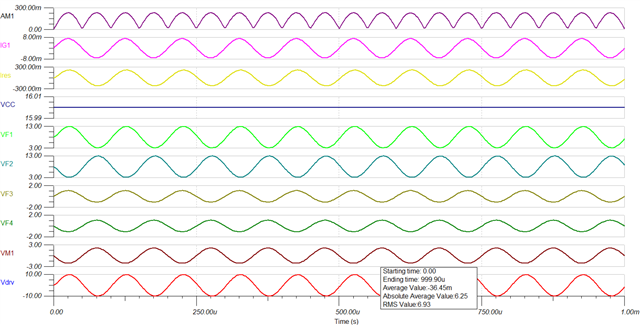
3. This design will be 7V RMS because we have bridge tied load excitation. You are correct that each amplifier will contribute 3.5VRMS excitation, we just tie resolver between OPA outputs, creating total 7V RMS:
See here, 6.93V RMS:

Here is new design for 10mA current and adjusted filter caps:

With our design, we have very stable operation:

Please let me know if you have any questions.
Best,
Jacob
Thank you, Jacob.
I have some additional questions.
1. Why has V1 changed from 15V to 16V, and why has R2 changed from 75Ω to 45Ω, with L1 being added?
I'd also like to know the reason why R14, R15 and C15 changed.
2. The OTF/SH_DN pins should be pulled up to 5V, right?
3. What happens if the AU6805 becomes the AUA6800?
That's all.
Hi Takaya-san,
I happened to use an older version of your design I had saved on my computer, this caused some values to change.
V1 can be 15V or 16V, no issue here. R2 and inductor are better representation of the resolver impedance. If you have a specific resolver you intend to use, I can swap it in place for accurate values.
R14, R15, and C15 have relatively small impact on the system. These divider resistors can be set anywhere from 1k to 100k, and the filter cap just helps ensure this node does not fluctuate or couple in HF noise.
My model does not include OTF/SHDN, but yes, this should be pulled up for active operation.
I am not finding the datasheet for AUA6800. Do you happen to have a copy to share? IN our case, we should really only care about how the excitation signal is being generated.
Thanks,
Jacob
Thank you, Jacob.
I'm sorry, but I only have the Japanese version. Is that okay?
If I want to share it, how should I do that?
That's all.
Hi Takaya-san,
I see. Yes, please share Japanese version, I believe I have translation tool which can help.
Alternatively, are you able to confirm if the AUA6800 is similar operation to the AU6805?
You should be able to insert the file like this:

Thanks,
Jacob
Hi Takaya-san,
Thanks for sharing this file.
It looks like the manufacturer has added additional features to this device, and these changes actually help our design.
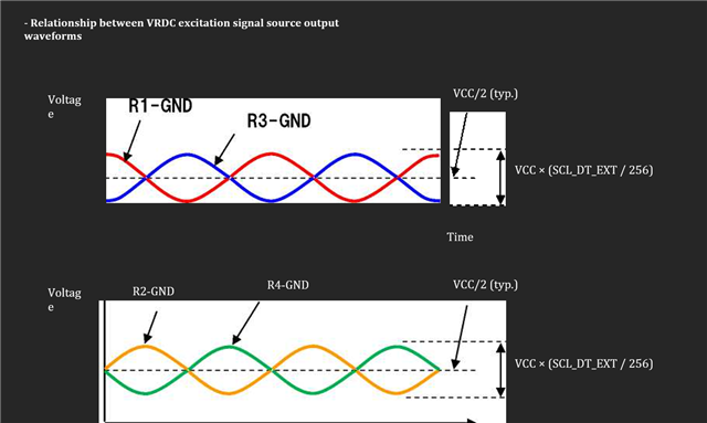
Now, we have 4 different sinusoidal outputs representing R1 - R4:
We can use either sine or cos output and also use the respective inverse phase output to create either of the following two waveforms

In our case, the schematic would not significantly change, though we would now not require a resistor between what was R1 and R2 on the AU6805.
It looks like the AUA6800 also has register adjustable excitation voltage which offers greater flexibility to your design needs.
Do you need help redesigning this circuit?
Thanks,
Jacob
Hi Takaya-san,
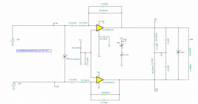
Here is the new design:

I have leveraged the new SCL_DT_EXT feature to allow you to fine tune your output amplitude. As is, I have the simulation running with an excitation of +-1.4V amplitude on the input (code 217), but the advantage is that you can change this number if you want more or less output signal.
To set this up, you would just connect R1 and R3 to the respective input terminals similar to my schematic.
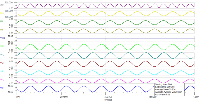
With this design, we have just over 7V RMS output with SCL_DT_EXT code 217.

Please let me know if you have any questions.
Please note, I will be out of office for the next two days. I may have a slight delay in responding to design questions during this time.
Thanks,
Jacob