This thread has been locked.

If you have a related question, please click the "Ask a related question" button in the top right corner. The newly created question will be automatically linked to this question.

XTR116: XTR116 Bypass Capacitor Placement

Part Number: XTR116

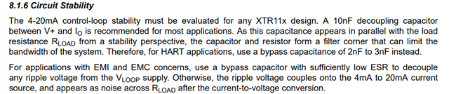
In the XTR11x datasheet, section 10.1 suggests connecting "low-ESR, 0.1µF ceramic bypass capacitors between supply pin and ground, placed as close to the device as possible". There's no 'supply' or 'ground' pin on the XTR11x chip. Is this just a piece of generic layout advice that was erroneously left on the datasheet, or am I missing something?

The datasheet also advises putting a 10nF decoupling capacitor between the V+ and I_o pins of the chip to help with power supply noise, but this seems like a separate thing from the bypass capacitor.


Thanks,

Tim

  • Hi Tim, 

    Thank you for pointing this out. You are correct, the recommendation is to apply a capacitor between V+ and Io for noise. The 0.1uF supply pin and ground statement was copied from a different datasheet.

    A 10nF capacitor is recommended for most applications, for HART applications, this can be reduced to 2nF or 3nF. 

    Best Regards,
    Ashley