This thread has been locked.

If you have a related question, please click the "Ask a related question" button in the top right corner. The newly created question will be automatically linked to this question.

TLV9152-Q1: OPA input short circuit analysis

Part Number: TLV9152-Q1
Other Parts Discussed in Thread: TLV9152

Hi teams,

I would like to ask about an unexpected behavior observed with TLV9152‑Q1 under an abnormal input condition.

OPA inputs IN+ and IN− (Pin5 & Pin6) are intentionally shorted together (fault injection / stress test).
This condition is understood to be outside normal operating conditions.


Observed Behavior
Two TLV9152‑Q1 samples show different behavior under the same test condition:
Sample A

With IN+ / IN− shorted:
OPA output / MCU I/O remains logic LOW
Behavior is as expected due to MCU pull‑down.

Sample B
With IN+ / IN− shorted:
OPA output (PIN7) / MCU I/O is pulled up to ~3.3 V (logic HIGH)
As a result, the MCU detects I/O as HIGH.

Verification Performed
To rule out MCU-related causes:
The series resistor R26 was removed, disconnecting the OPA from MCU.
Result:
Both samples show identical MCU behavior.
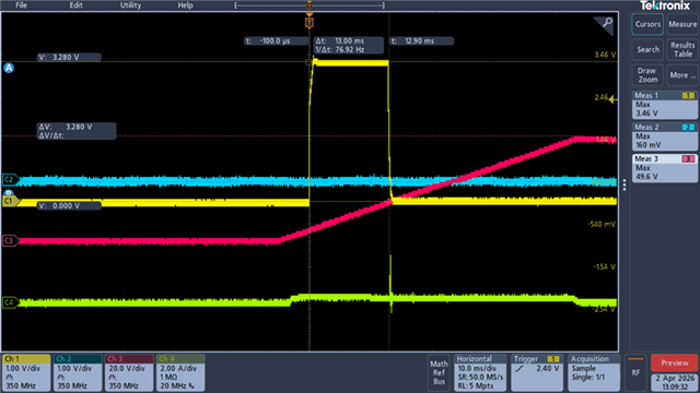
MCU I/O pin briefly goes HIGH (~20 ms) during MCU power‑up, then is pulled LOW by the internal 100 k pull‑down.

This confirms:
MCU reset / firmware / internal pull configuration is not the source of the difference.
The difference only appears when TLV9152‑Q1 output is connected.


Questions

Why do these two samples exhibit different behaviors?
Is this difference caused by sample‑to‑sample variation in the op‑amp output current when the inputs are shorted, resulting in one MCU IO being pulled above VIH (logic HIGH) while the other remains below VIH (logic LOW)?
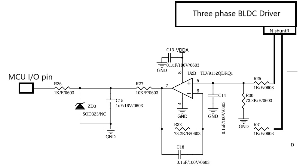
 image.png

  • Hi Chia Chieh Lin,

    Yes, the difference between the samples is most likely caused by sample-to-sample variation. When the input pins are shorted together, the input offset voltage of the amplifier will cause the output at pin 7 to swing either high or low, depending on the polarity of the offset voltage. 

    Let me know if you have any questions Slight smile

    Best Regards,

    Alex Curtis

  • Hi Alex,

    This waveform is remove R26 and measurement MCU I/O pin (CH1). When MCU wake up, the I/O pin output the ~20ms pulse. 

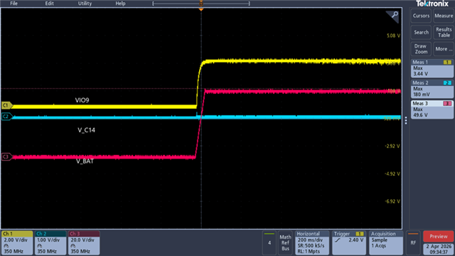
    This waveform is put R26 back and measurement MCU I/O pin (CH1), why the waveform does not same as above CH1(~20ms pulse)?

    It's seems like OPA output be pulled high to 3.3V. 

    When I change OPA, the MCU I/O pin(CH1) does not pull high to 3.3v. 

    Is the OPA characteristics?

    Thank you.

  • Hi Chia Chieh Lin,

    Thank you for the scope captures. To make sure I understand, please confirm that my interpretation of the images is correct:

    1. Image 1 shows the MCU pin when the MCU wakes up (R26 removed, op amp output disconnected)
    2. Image 2 shows the MCU pin when the MCU wakes up (R26 populated, op amp output connected, amplifier A)
    3. Image 3 shows the MCU pin when the MCU wakes up (R26 populated, op amp output connected, amplifier B)

    Please clarify the following details about your test setup:

    1. What is the supply voltage of the op amp (VDDA)? 
    2. Is the supply to the opamp enabled for the full duration of the test?
    3. Are the inputs of the amplifier shorted together at pin 5 and pin 6 in all 3 measurements
    4. Is the shunt resistor connected during the tests? If so, what is the shunt resistor value?
    5. Other than R26, is the circuit populated with all components shown in the schematic during the tests?
    6. Is the Zener diode populated? If so, what is the part number?
    7. What is VBAT?
    8. In the first image, what is channel 4 (Green) measuring?

    Next steps:

    With R26 removed (MCU not connected) and pin 5 and 6 shorted together, do the outputs of both amplifier A and B (pin 7) stay at ~0V? 

    Best Regards,

    Alex Curtis