OPA564: Power‑up sequence for the OPA564AIDWP

Part Number: OPA564

Could you please advise on the power‑up sequence for the OPA564AIDWP?

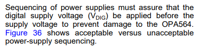
According to the datasheet (page 14), the specified sequence is to power up Vdig first, followed by Vsupply. However, since the Vdig supply is referenced to the V− rail, would it be more appropriate to power up in the order V− → Vdig → V+?

Alternatively, should the sequence be Vdig → V− → V+, or Vdig → V+ → V−?

Additionally, are there any specific requirements or constraints regarding the power‑down (power‑off) sequence as well?


image.png

image.png

  • Hello, 

    You are absolutely correct. The datasheet covers single-supply configuration, though split supply is the real point of concern. 

     V− → Vdig → V+ Is correct in some cases, though this depends on supply voltages. 

    As you correctly identified, we have a supply voltage limit for the Vdig connection, referenced to V-:

    Where this gets a bit strange is the fact that I need to ensure Vdig never exceeds 5.5V from V-, even during startup. Lets say you want to use +-12V for example:

    In this case, we need to be very cautious for how we set up this circuit. VDIG in this circuit will actually be negative, and we can sequence at the same time as V-. For valid operation, we need to be between [ (-12V - -5.5V) to -12V - -3V)] = [ -6.5V to -9V ] .

    This is how the sequencing could look:


    I complete both conditions: 

    1. Vdigital never exceeds 5.5V.

    2. Vsupply is controlled to ensure Vdig does not change too late on startup, or too early on ramp-down

    In my simulation, VDIG represents the waveform sent by the circuitry that will bias the OPA564. Vdigital represents the equivalent single supply voltage seen by the VDIG pin referenced to V-. Note, VDIG must be a negative voltage relative to GND to allow for this operation to work. 

    In reality, it may not always be possible to ensure that your V- supply and Vdig ramp at perfect rates and times. In these scenarios, I might recommend placing a clamping diode between the rails to help ensure the VDIG is not in violation of the datasheet. Alternatively, you could always make Vdig derive from V-, helping ensure that Vdig is presented at a similar rate to V-.

    What are your application requirements here? I just want to make sure OPA564 is the best fit for your application. 

    Please let me know if you have any questions. 

    Best,

    Jacob

  • Thank you very much for your valuable advice.
    Please accept my sincere apologies for the delay in my response, as we were conducting evaluations using the actual hardware.
    After careful consideration, we have decided to generate the Vdig power supply using the Zener diode you recommended.
  • In addition, we have one additional point we would like to clarify.
    When using the OPA564 with a ± power supply, should the 0.1 µF capacitor for the Vdig supply be placed between Vdig and V−, or should it be connected between Vdig and the board GND?
  • Hello, 

    Thank you for considering to implement Zener based power supply. 

    Good question on the power supply bypassing. Return current s from Vdig will be small, so either could be selected as the termination for the .1uF cap. If you have an uninterrupted V- plane on the board, I would use this as a termination for the .1uF cap. If you do not have a large V- plane, GND works perfectly fine for decoupling. 

    Please reach out if you have any questions on the design,=.

    Best,

    Jacob