This thread has been locked.

If you have a related question, please click the "Ask a related question" button in the top right corner. The newly created question will be automatically linked to this question.

PGA849: LVDD LVSS /Vsout Current Consumption

Part Number: PGA849
Other Parts Discussed in Thread: PGA848, , OPA192

Hi TI,

There are 2 questions actually:

  1. Looking at the quiescent current plot, it's about 4mA at 25degC:image.png
    and the table spec is: image.png
    I take the plot as the sum of input and output stage supplies, as the input supply is just 3mA typ. But from the table spec, they sum up to 5.3mA typ, which is quite different than the 4mA from plot. Which number should I use for calculation in my design?
  2. I really like the plot of current consumptions vs input differential voltage as it helps me to estimate the current consumptions.
    image.png
    Does TI have one for Vsout as well? That would be very helpful to estimate the total current during overdrive.

-Hao Jie

  • Hello Hao Jie, 

    Regarding the quiescent current on the PGA849, the datasheet is incorrect in the electrical characteristics table and will be updated in the next revision of the datasheet.

    The correct current consumption on the output stage will be a lot closer to what is seen in the PGA848's datasheet: 

    If we take that into consideration, Figure 6-62 makes a lot more sense. The label "input stage" will also be removed as that is current consumption for the input and output stage. 

    For the second question, Figure 8-6 includes both the current consumption on the input and output stage as the VS=VSOUT=±15V.
    If you would like to confirm the specific power supplies used in your application and what sweep of differential input voltage you are interested in seeing, I can test this on the EVM. 

  • Thanks for the clarification, that PGA848 consumption is closer to 4mA.

    For the sweep, I would be using closer to ±14V, but Vref could be at 2.5V, can you do the same sweep up to ±30V?

  • Hello Hao Jie, 

    Yes, I will measure this on the EVM, are you interested in multiple gains or only in a gain of 1V/V? If the VREF is 2.5V, what would like the VICM to be? 

    All the best,
    Carolina

  • Gain of 1V/V is enough, since this has the highest consumption. VICM of 0V is good enough.

    Thanks!

  • Hello Hao Jie, 

    The PGA849EVM has two ways of connecting a reference voltage, externally with a power supply or through an op amp (OPA192 in this case). I provide both of these as the reference buffer is necessary if providing the reference voltage from a low impedance source (resistor divider). 

    Here is the PGA849 with the REF voltage provided from a power supply: 

    Here is the PGA849 with a REF voltage provided through the OPA192, note on the EVM the OPA192 is also powered by VS: 

    I included both as I expect the second scenario to be the more in line with a real application. 
    I also included reference lines that show where the limits are for the max/min differential input voltage for linear operation. If you are unfamiliar, please use the calculator available on ti.com. 

    All the best,
    Carolina 

  • Carolina,

    Thanks for making the measurements! This information will be really useful in estimating the power consumption.

    I have one question though, now the quiescent current when Vin = 0V, is significantly higher than the datasheet, Vref = 0V case.

    Since the output stage resistors are 5kohm each, I don't think it's because of the change in Vref. Do you have more insights into this?

  • Hello Hao Jie, 

    I am not sure, let me take a couple more tests. 

    All the best,
    Carolina

  • Hello, 

    Slight update, I tried to recreate Figure 8-6 in the datasheet and it was higher than what I expected.

    I removed the TVS surge protection diodes and it improved a little bit.  

    It is still not as low as I would expect: 

    Next I removed the Schottky diodes: 

    As you can see it didn't improve by much and I applied a large differential input to the device when it wasn't powered. 

    My next step is to replace the device and continue testing, this will take some time as I had to order some PGA849s. 

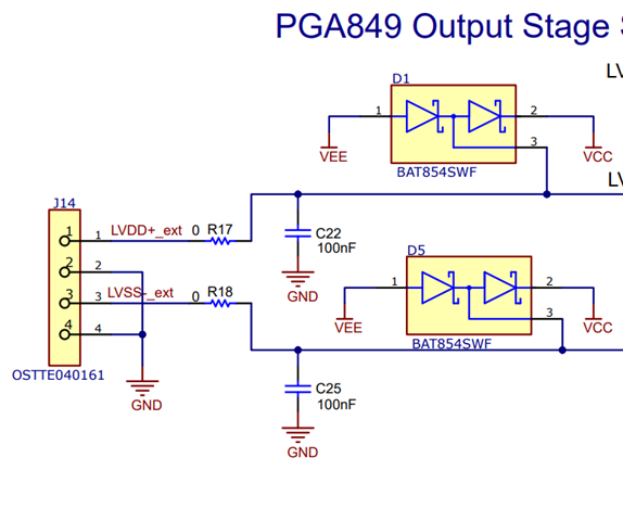
    In the PGA849EVM user's guide is the schematic (page 11), let me know if there is anything else you suspect might be consuming current. 

    I think overall the data provided earlier is the most accurate current consumption of the PGA849 implemented. The design is most robust with the diodes that I removed, it helps protect against surge electrical overstress events. 

    It is also possible that this PGA849 is just a higher Iq device on the statistics curve (2.2mA + 4.6mA = 6.8mA). My measurements are done at room temp but I wonder if violating the linear operation region and using the OVP heats the device. 

    I will report back when I have more results. 

    All the best,
    Carolina

  • Sorry I didn't get the notifications earlier. Was the divider current, Vref buffer current, and the gain setting resistor current accounted for? Maybe they are the extra loading.

  • Hi Hao Jie, 

    Good thinking! The VREF op amp was removed but the surrounding passives were still populated. I will remove those and see if I can get performance matching the datasheet. 

    All the best,
    Carolina

  • Hello Hao Jie, 

    I removed a lot of things from the circuit (even the output loads and everything associated with the output), not much changed.

    I was finally able to get something resembling what is in the datasheet, it meant that I had to power the input and output stage power supplies from different sources (still the same value) and only measure the power consumption of the input stage instead of the power consumption of the whole device.

    Please see results: 

    As stated earlier, for your power budget, I would use the results from May 8th as I think that is more representative of the true application of the device. 

    All the best,
    Carolina