This thread has been locked.

If you have a related question, please click the "Ask a related question" button in the top right corner. The newly created question will be automatically linked to this question.

TLV3901: Comparator Output Behavior Clarification

Part Number: TLV3901

Hi Team,

Posting on behalf of our customer.

I'll share this E2E post with our customer so he can reply when needed.

We are currently evaluating your comparator and observing some unexpected output behavior. We would appreciate your support in understanding the issue.

In our design:

  • VCCI = 5.2 V
  • VCCO = 3.3 V
  • VEE = Ground
  • Hysteresis pin is connected to ground through a 750 Ω resistor (as per datasheet, expected hysteresis ~20 mV to 30 mV)
  • LE pin is connected to ground through a 470 Ω resistor.
  • LE/ pin is left unconnected
  • VTP and VTN pins are left open.

Observed behavior:

  • Case 1: VP ≈ 0 mV, VN ≈ 50 mV
    Output: QP ≈ 3.17 V, QN ≈ 3.13 V
  • Case 2: VP ≈ 91 mV, VN ≈ 106 mV 
    Output: QP ≈ 3.19 V, QN ≈ 3.11 V

Ideally, we expect a clear differential output as mentioned in the datasheet, but both outputs are nearly at the same level.

Regards,

Danilo

  • Hi Danilo,

    How are these nodes being probed? Are you able to share some oscilloscope waveforms or schematics? How do the outputs look if you increase the input differential?

  • The current measurements are for DC Levels. We are validating first the static performance of chip. There is no need for waveforms, even in the scope it is straight lines. Once we get the static measurement proper then we will moving towards dynamic performance of chip. The data we have given is very detailed and self explanatory. 

  • Hi Bhoomika,

    Thanks for clarifying that you are doing DC tests here. I read over your design circuit, but there isn't anything there that is readily pointing to why you are observing the outputs not fully swing differentially. As such, I need to ask some clarifying questions on my end to fully understand the set up and to debug this issue. 

    Are you using the TLV3901EVM to run these tests? If not, please share a schematic of the board you are testing the TLV3901 with.

    I want to confirm the output load on Q and Q/. CML outputs operate by steering ~16mA across resistors connected to VCCO. Please see below:

    Comparator Output Types

    The swing will change depending on the loading of the outputs.

  • We will explain the circuit below again. 

    TLV3901 :  VCCO is connected to 3.3V, VCCI is connected to 5.2V, VTN and VTP are floating. We have provision to connect  0V or 91mV at VP input. We have a provision to change VN from 0V to 200mV [ Using a DAC] . We have connected LE pin is connected to ground through 470 ohm and LE/ pin is floating. Hysteresis pin is connected to ground via 750 ohm.

    The outputs QN and QP are connected to HMC746LC3C inputs. HMC746LC3C is a device supporting CML logic levels with inbuilt 50 ohm termination to VCC. We are loading TLV3901 at the digital output as per CML guidlines.

    The issue we had raised earlier that QP and QN are not at proper CML logic levels as explained earlier, remains as a question to be answered .

    If the device really supports hysteresis, QP and QN shall be either less than 2.9V or close to 3.3V depending on the logic level. The voltage level like 3.15V is not correct. We are asking for clarification on this.

    We will also appreciate if you can clearly explain the hysteresis as supported by TLV3901 [The device is not working as per the hysteresis, expected normally] . The device seems to be having a design problem when the voltage difference between VN and VP is below some level and defenitly below 40mV. 

    We will appreciate if TI can investigate thoroughly the hysteresis capability of TLV3901 and let us know if there is any problem.

    The analog device part ADCMP572 defines a parameter called Gain  (more than 50db). Does TI have any test result for the Gain.

    We will appreciate if you can look at our inputs seriously, give sufficient thought, discuss with design team of TLV3901 and provide us with a clear technical answer.

    Please let us know whether there is any errata sheet or  performance deviation note published by TI for TLV3901.

  • Bhoomika

    Thanks for your patience as we try to resolve the issue.  I am sorry that you feel we are not treating your post seriously.  Unless the device has been damaged, we agree that we see no issue with the setup you describe.  Since you provide no images of the setup, we will just have to accept the conditions as described.  Most customers simply share their schematic and waveforms as it makes things much easier. 

    What is the supply current from VCCI and VCCO (understand that both VEE are connected to GND)? We would like to compare our EVM configured exactly as yours is.  Since this is a leadless package, are you using a socket or did you solder it down onto a PCB you created?  if soldered down, was it hand soldered or machine soldered?  

    The only thing I don't see in your description of downstream device is what is VCC of HMC746LC3C connected to.  I assume itis the same 3.3V as you mention for our VCCO.  As a trouble shooting option, have you tried to look at the TLV3901 output without the HMC746LC3C connected.  I am just trying to rule out any factors other than the TLV3901.  Since the output simply steers 16mA through the internal (50 ohms) and external (50 ohms) for total of 25 ohms in parallel, I can't imagine how you would get anything other than close to 400mV swing on each output, unless device is damaged or not properly soldered down.

    Lastly, is the issue only observed on one device?  Any chance you can get an EVM from us to experiment with?

    Chuck

  • The downstream device HMC746LC3C is powered with 3.3V. This being a CML device the power supply should be  typically 3.3V. We have assembled 3 cards with TLV3901,directly source from Texas Instruments. All are behaving the same way. All the cards were assembled in a automated assembly facility. 

    We strongly believe that the Ti device has a fixed gain from input to output. The hysteresis do not seem to be implemented in the standard way. The best analysis going forward, in my opinion is as follows.

    Please use your evaluation board and please try out the following tests:

    1. Apply a differential voltage between VP and VN of 25mV, 20mV, 15mV, 10mV and 5mV in the EVM. Please observe the outputs QP and QN.

    We think, based on our observations, you will observe  both QP and QN to be around 3.15V and not have 400mV difference. The idea is to qualify TLV3901 for small differential inputs.

    2. If you observe more than 400mV difference between QN and QP, we can proceed from our side with more observations as you suggested, like Isolating HMC746LC3C connection (ours is a high density board and disconnecting from QN,QP will mean desoldering the HMC746LC3C device).

    Regards

    Bhoomika M H

  • Hi Bhoomika,

    I just wanted to update you on this issue. The current results we are seeing in the lab are inconclusive. We'll get back to you with an update tomorrow.

  • Hi Bhoomika,

    Please give us some more time to review with our designers.

  • Hi Bhoomika,

    Thank you for your patience. I've personally gone ahead and conducted some experiments with the TLV3901 in the lab.

    For the following tests, I connected the TLV3901 with the following operating conditions:

    VCCI = 5.2V

    VCCO = 3.3V

    VEE = VTP = VTN = VN = GND

    HYS = 750Ω to VEE

    LE_N = Floating

    LE = 2.9V

    VP = Swept by DC power supply

    There is no external termination at the outputs of Q and Q_N.

    I began sweeping the VP voltage with the DC power supply, and probed both VP. Q, and Q_N with a digital multimeter. Below is the table of my DC readings.

    VP Q Q_N
    98.9mV 3.285V 2.528V
    49.1mV 3.285V 2.528V
    9.2mV 2.930V 2.875V

    Using the same configuration, I connected the outputs Q (Channel 2) and Q_N (Channel 1) to a 500MHz BW oscilloscope. I swept the VP from 50mV to GND, and I obtained the following scope shot as the outputs transitioned:

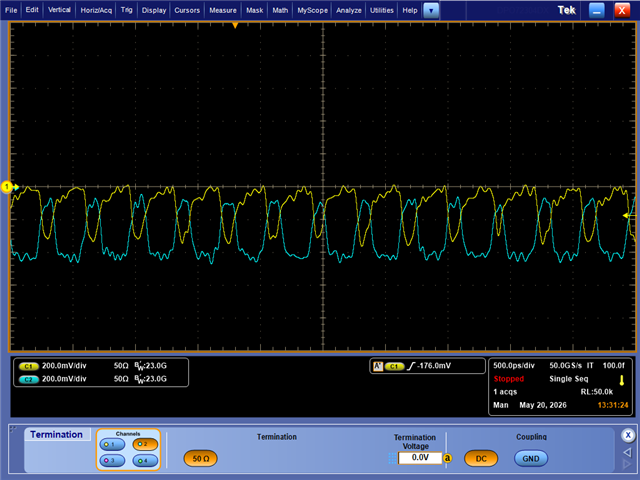
    For the next test, I connected the outputs Q (Channel 2) and Q_N (Channel 1) to a 26GHz BW oscilloscope. This time, there is an external 50Ω to VCCO from the oscilloscope (high speed scopes do not allow for high impedance inputs). Please also note that the 0 level on the waveform is VCCO. Once again, I swept VP from 50mV to GND until the waveforms collapsed from a clean CML differential:

    As you can see, there is significant chattering at the output between VCCO and VCCO - 400mV, and it's not stuck at some mid-CML level.

    What is most likely happening in your DC tests is that you don't have a clean differential between VN and VP. Noise from your VN/VP drivers as well as interference from your environment are causing the VN and VP channels to cross and exceed the configured hysteresis. This causes the output to chatter at a very high frequency.

    The mid-CML level you are reading in your DC test is due to the low-pass filtering effect from the bandwidth of your test equipment, and you are reading an average voltage in both Q and Q_N that level out at around 3.15V.

    As you can see in the first two tests, the chattering is wholly undetectable by the DMM and the 500MHz BW scope; they both interpret the outputs to be some DC mid-CML voltage when in reality the outputs are toggling at a very fast rate.

    To mitigate this chattering, you can increase the hysteresis of the TLV3901 by shorting HYS to VEE or alternatively clean up your VP and VN signals.