This thread has been locked.

If you have a related question, please click the "Ask a related question" button in the top right corner. The newly created question will be automatically linked to this question.

AMC3302: conducted emission

Part Number: AMC3302

Hello,

In our design, which we created following the application note "Best Practices to Attenuate Radiated

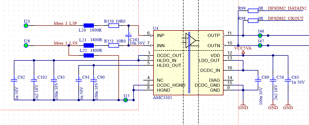
Emissions EMI," which we created using ferrite beads, we have identified a problem with conducted emissions. Our measurement results vary with each measurement. We suspect that interference is coupling through the ferrite between the HGND and INN. Have conducted emission measurements been performed by TI? How can we resolve this issue?

Greetings, 

MarcelAMC3302.png
  • Hi Marcel, 

    Can you please provide the layout and conducted emissions results of this design? 

  • Good Morning Alexander, 

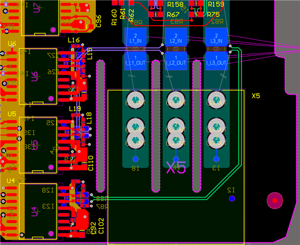
    i can only give you a screenshot of the Layout, U4,U5,U6 these are responsible for current measurering. If you need more detailed layout information i can provide you that.

    The measurement results show that the analog voltage at the shunt fluctuates significantly as the frequency increases. We did not record these measurement results.

  • Hi Marcel, 

    Do you mean the analog measurements from these devices, or the conducted emission result changes? 

    If the analog measurement is what is changing, are you suspected that it's a result of the conducted emissions? 

    Which ferrite are you using? 

    For analog measurements: In general I wouldn't expect the conducted emissions to impact the measured results at the device has a bandwidth of ~300kHz, while the emissions will be in the MHz range, so your anti-aliasing filter and the inherent gain/frequency characteristic of the device should properly attenuate this noise.  Since you have three parallel sensing channels however, I recommend considering crosstalk. Do you have the ability to turn on current on one channel in a lab setting, while measuring all three? 

    For conducted emissions: We would want to consider modifying the layout with some blue-wires to test a few things. It's possible there is coupling between traces that is reducing the effectiveness of the ferrites as currently laid out. I wouldn't expect this to change significantly run-run however. 

    Please help clarify the issue so I can further assist. 

  • Hi Alexander, 

    yes we were able to observe that the conducted emission affected our analog measurements. Normaly we have a stable analog measurements with HGND tied to INN but if we place a ferrit bead as suggested in the application note from HGND to INN the measurement is showing false results at conducted emmision. 

    We are using Würth 74269244182.

    One channel was already under load during our measurements.

    We'd be happy to make some improvements to the layout—what would you suggest?

  • Hi Marcel, 

    Can you please provide an example of the conducted emission affecting the analog measurement? Is it channel to channel dependent? 

    Sensing connection to the shunt should be in the middle of the pad, often as shown in the shunt datasheet. 

    Typically we recommend routing the HGND to the shunt as well, as shown in figure 3-4 of the application note you reference. 

    Pin 2-8 connection should be prioritized on the top side of the PCB, also as shown in layout of the application note. 

    There are traces after the ferrite bead, that route back under traces/planes near the IC, this would allow capacitive coupling to bypass the ferrite bead.