This thread has been locked.

If you have a related question, please click the "Ask a related question" button in the top right corner. The newly created question will be automatically linked to this question.

INA381-Q1: Technical questions

Part Number: INA381-Q1

Hi team,

I have technical questions regarding INA381A1-Q1. Could you please kindly help me answer?

  1. My customer would like to add the capacitor between IN+ pin and IN- pin to suppress the high frequency noise. Is it possible to do it? The user guide of EVM shows the capcitor is connected between IN+ pin and IN- pin.
  2. If yes, what is the recommended value of the capacitor?
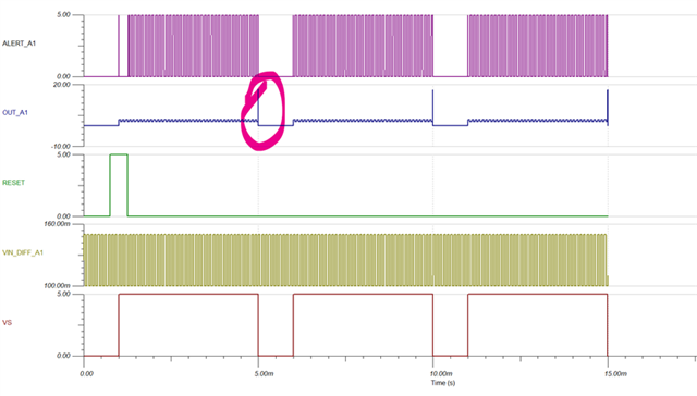
  3. My customer simulated the PSpice model of INA381A1-Q1. The voltage of VOUT pin becomes 17V at maximum when the power supply to VS+ pin is off. I have attached the simulated waveforms and the simulated circuit below.
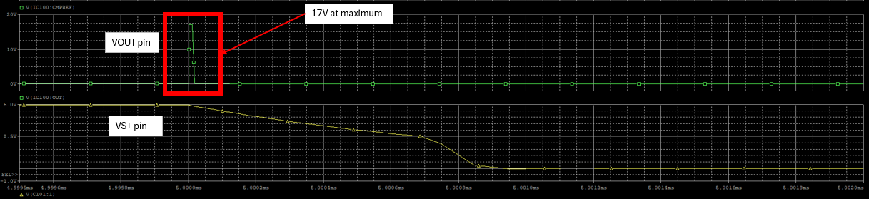
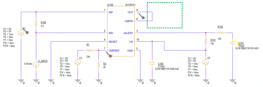
image.png

image.png

4. The output voltage of VOUT pin exceeds the abs max of OUT pin which is 5.3V when power supply of VS+ pin is 5V. In this case, the voltage of VOUT pin gets clamped to 5V or the IC gets broken due to the violation of abs max of VOUT pin?

image.png

5. If the voltage of VOUT pin doesn't get clamped to 5V, is it acceptable to 5V zener diode to clamp the output voltage of VOUT pin?

6. Are there any ways not to output the comparator(ALEART pin) during the power on and power off? My customer is looking for the feature which disables the output of the comaparator(ALEART pin).

Best regards,

Shunsuke Yamamoto

  • Yamamoto-san,

    Thanks for the question and using the E2E forum.

    My customer would like to add the capacitor between IN+ pin and IN- pin to suppress the high frequency noise. Is it possible to do it? The user guide of EVM shows the capcitor is connected between IN+ pin and IN- pin.

    Yes, the customer can add a capacitor between the inputs, and we specifically show this scenario in section 8.1.4 in the datasheet.

    If yes, what is the recommended value of the capacitor?

    This would depend on what frequencies the customer is concerned about. We have a good FAQ (good information that pertains to this question even though it was written for a different device) as well as a TIPL that helps in designing these input filters.

    The output voltage of VOUT pin exceeds the abs max of OUT pin which is 5.3V when power supply of VS+ pin is 5V. In this case, the voltage of VOUT pin gets clamped to 5V or the IC gets broken due to the violation of abs max of VOUT pin?

    I am waiting on some information from our design team about an internal clamp. I don't think the 17V on Vout is realistic and may be a glitch in the model, but I'll update here once I receive further information.

    Are there any ways not to output the comparator(ALEART pin) during the power on and power off? My customer is looking for the feature which disables the output of the comaparator(ALEART pin).

    There is not a way to enable/disable the ALERT pin on this device.

    Please let us know if you have any other questions.

    Louis

  • Yamamoto-san,

    I have confirmed with our design team that the output is internally clamped to avoid it going much higher than supply.

    Looking at the simulation, it really looks like it's an artifact of the simulation itself.

    Rerunning the simulation, we see the same spike...

    It appears to be coming about from the customer’s setting of “0ms” rise and fall time. There has to be some realistic value of rise and fall time, or else the system doesn’t know what to do. If we update this to even 1ns, the artifact disappears...

    Please let us know if you have any other questions.

    Louis