This thread has been locked.

If you have a related question, please click the "Ask a related question" button in the top right corner. The newly created question will be automatically linked to this question.

Switched Capacitor Amplifier

Hi,

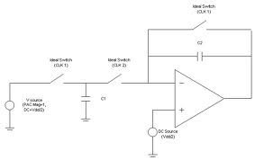
This is Jyothi, an MTech student from India. We are trying to design a switched capacitor amplifier with gain of 100 . We have done a normal inverting amplifier  using opamp and resistors (Ri=1kohm and Rf=100kohm) and we are getting the output. But once we replace all resistors with switched capacitors, we are getting some weird output. Our input is a sine wave of frequency 1MHz and peak-peak amplitude 2mV centered around 2.5V and the frequency of non-overlapping clocks is 2MHz. Our supply is 0-5V. What could be the issue? We are unable to fix it. What is the kind of output that we should expect. Please help. Could you kindly share a commonly used SC Amplifier circuit. We are trying to simulate the circuit in HSpice. Please find the attached for the circuit we are using.
Thanks,

Jyothi

  • Hi Jyothi,

    There are a few problems I see which could be preventing proper operation of your circuit and,as you may have found, simulating switching circuits like yours tends to cause convergence issues. To start, for switched capacitor operation to be considered continuous (in other words for the switched cap to properly act as an equivalent resistance) the clock frequency must be much higher than the signal frequency. If you wish to pass a 1 MHz sine wave I would not use a clock frequency slower than at least 10MHz. This raises another concern, are the switches you are using able to switch at this speed? MOSFETs capable of switching at this speed may have a significant on-resistance which will slow the capacitor charging and may produce unexpected results. The parasitic capacitances of these switches may also effect the accuracy of your equivalent resistance calculations. It is unlikely that you will be able to prototype a circuit switching at this rate without a well laid out printed circuit board.

    You will need to select an operational amplifier that does not have back to back diodes across the inputs as these will short out the voltage across the capacitor when it is connected to the input. Also, I believe you will require a second switch in the feedback loop to properly act as a resistance as I have shown below:

    In some of my own simulations I used 100kHz non-overlapping clocks for a signal of 1kHz, and I also employed an RC low-pass filter at the output of the amplifier to remove the switching noise.

  • Thanks John,

    We tried with the circuit diagram you had shared. We are getting some output, but wanted to verify if its correct. Before that, we had a doubt on how to select the C1 & C2 values. Our understanding is that Ceq=T/R, where T is the clock period of non-overlapping clocks. Is this understanding correct? With this, we calculated our C1=C2=10nF(for R=1Kohm). With this and different values of C1 & C2, we simulated and we got different outputs. Please find the attached for the waveforms.

    Our input is a 1Khz sine wave of pk-pk 1V centered around 2.5V as we have a supply of 0-5V. The non-overlapping clocks are of frequency 100Khz as you have mentioned.

    Also if we need to get a gain of above 1000, what values of C1 & C2 we should use? We understand gain = C1/C2. Is this correct? Also what is the maximum gain that can be achieved by a single stage?

    If the waveforms are wrong, can you please send us the expected waveform of your circuit.

    Regards,

    Jyothi

  • Hi,

    Can you please verify the answer. We are stuck here and do not know how to proceed. Please help!

    Regards,

    Jyothi

  • Jyothi,

    Did you incorporate the RC lowpass filter that my schematic had on the output of the amplifier? This will reduce the switching noise in the output and make it easier to confirm proper operation. Remember that your equation for the equivalent resistance is accurate as long as the capacitor has sufficient time to charge through the on-resistance of your switch. The maximum gain achievable by a single stage is determine exactly the same way as it would be for a regular opamp, with the major constraint being bandwidth, but you must also consider what values of capacitance are practical.

  • HI John,

    We had used the lowpass filter, but the output we shared with you is the one before the filter, as after filter we were getting a very weak signal as output.

    Our capacitance value is 10nF which is sufficiently less. Could you kindly share the output you have obtained with the same circuit so that we could verify our output. Our input is a sine wave of pk-pk 1V centered at 2.5V and supply is 0-5V and frequency of input is 1KHz and non-overlapping clock frequency is 100Khz. We have used a ideal switch modelled in Hspice with Ron=0.1m.

    Thanks,

    Jyothi

  • Jyothi,

    Playing with my simulations here I believe one of the main issues with this circuit is that the switching frequency is still within the bandwidth of the opamp. Therefore the amplifier attempts to amplify both the input signal and the switching noise. Choosing an amplifier with a lower bandwidth, or a switching frequency well above the amplifier's bandwidth should help with some of the switching noise on the output.

  • Hi John,

    On simulating with certain values of capacitors, we have obtained the following waveform and also we have obtained gain of 250 for a gain designed for 500. Attached is the waveform. Please let us know if this output looks fine.

    We tried to cascade one more stage to obtain more gain, but then this leads to distorted output. Is cascading not possible for Switched Capacitor?

    Thanks,

    Jyothi