This thread has been locked.

If you have a related question, please click the "Ask a related question" button in the top right corner. The newly created question will be automatically linked to this question.

INA333: Problem with gain

Part Number: INA333
Other Parts Discussed in Thread: TINA-TI

Hello,

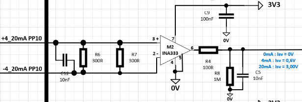
I use an INA333 with V+=3V,3 V-=0V, Rg=NC and Vref=0V

Vin+ and Vin- are connected to a shunt wich is isolated of the 0V

The output at Vout pin is not correct

Point 1 : Vin+ - Vin- = 0,6V and Vout = 0,4V instead of 0,6V waited

Point 2 : Vin+ - Vin- = 3,0V and Vout = 2,75V instead of 3,0V waited

  • Hi Pierre,

    You mentioned the difference between the Vin+ and Vin- but what is the input common mode voltage? 

    Best Regards,

    Robert Clifton 

  • I use this setup. I don't put resistor or capacitor between Vin+ and 0V or Vin- and 0V. They are missing ?

  • Hi Pierre,

     I think what is happening is a limitation of the boundaries. I'm using the Analog Engineer Calculator tool to determine this. For my calculations, I assumed that the inverting input is grounded and the positive input is the one that's seeing the voltage shift. 

    For the 4mA case, I assume IN- = 0V, and IN+= 0.6V. That would put the common mode voltage to be at 0.3V. Plugging in the values to the calculator tool, I see that the maximum output voltage that the INA333 can produce is at 0.4V, which appears to be what you are seeing.

    For the 20mA, that assumption would mean that for IN- = 0V, and IN+ = 3V. That would put the common mode voltage to be 1.5V. Plugging in the values to the tool, I see that the maximum output voltage that the INA333 can produce is about 2.8V. That matches very closely with your 2.75V output. 

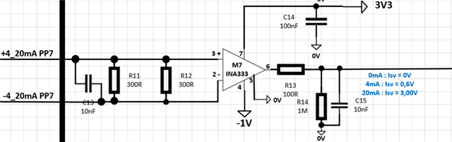
    How do you fix this? Well we can either change the reference voltage, change the input common mode voltage, or change the supply voltages. Let's just change V- = -1V. Now as you can see from both previous test conditions, the output can drive to the voltages that you are expecting. 

    Let me know if anything is unclear or need any more help! 

    Best Regards,

    Robert Clifton 

  • Hi, if i understand; i need to put a negative voltage on V- pin (-1V for exemple).

    I must to let Vin- pin like my scheme.

    And, i'll connect Ref pin to 0V

    Can you check in your simulation if this case is compliant with my request

    Thans

  • Hi Pierre,

    I must to let Vin- pin like my scheme.

    I'm not sure what exactly you mean by this but here's the results that I got with Tina-TI simulation:

    INA333 Gain problem.TSC

    Please note that the TINA-TI model doesn't have as robust of a boundary plot as the analog engineer calculator tool. That's why I recommend testing in the tool for boundary related concerns. 

    Best Regards,

    Robert Clifton