Part Number: THS4503
Good afternoon,
I am developing a mixed signal PCB which implements the ADC LTC2291.
I have selected the THS4503 as the driver of the ADC, and after trying to simulate the settling time using TINA TI i have stumbled upon a problem i can not seem to solve.
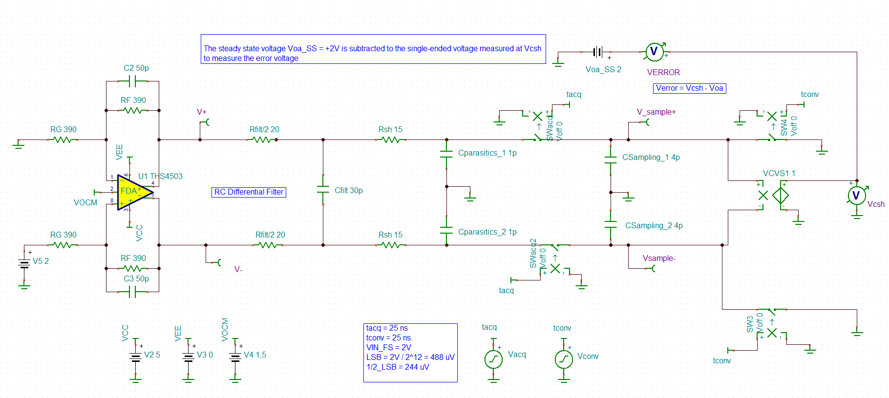
I sized the differential RC filter to comply with the acquisition time (tacq = 25ns since my fs = 20 MHz) setting the maximum allowable error to 1/2 LSB = 244 uV as my VFS = 2V.
The THS4503 is configured with gain = 1v/v and utilizes feedback compensation capacitors.
To simulate the settling time i have followed the TI-Precision Labs series on FDAs.
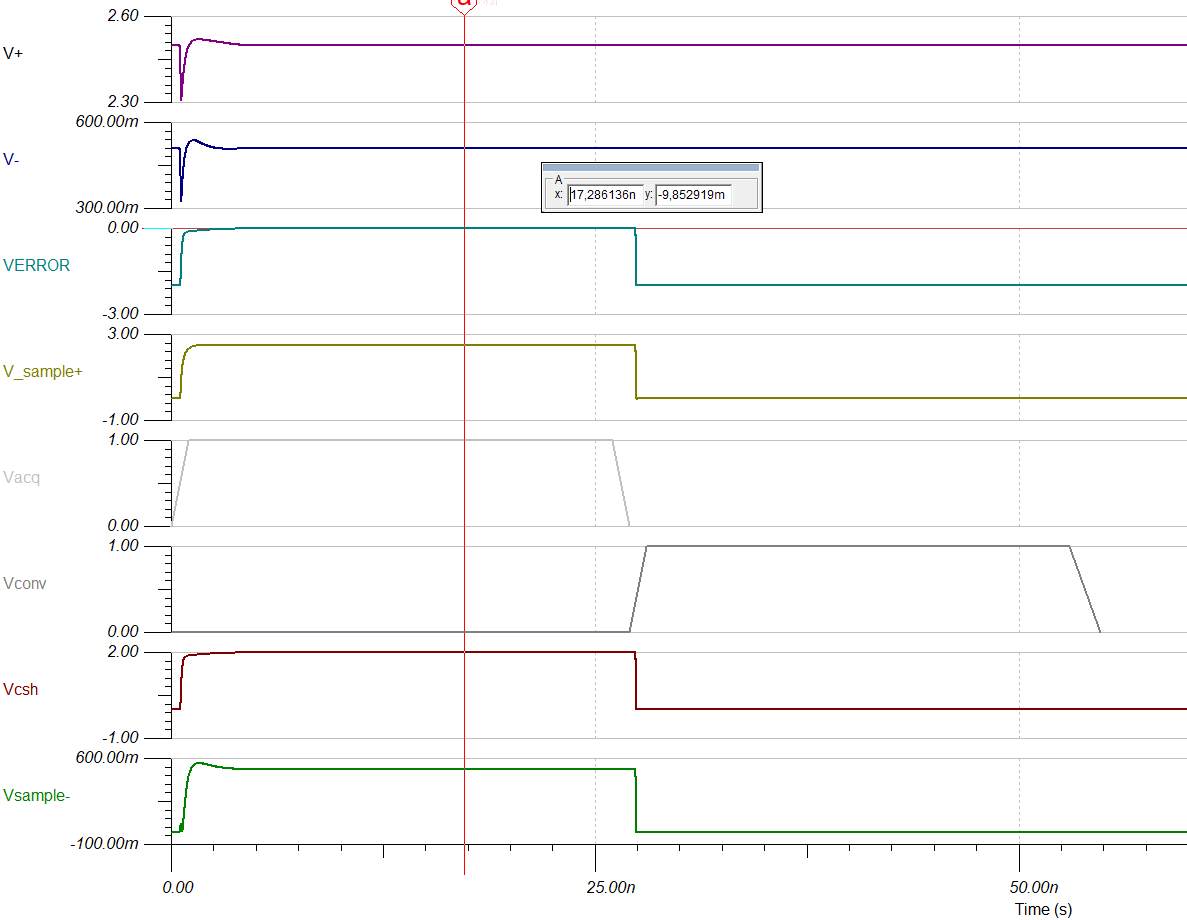
My simulation consists on feeding +2v DC voltage to the non-inverting input of the THS4503 with VCC = +5V, VEE = 0V and VOCM = +1.5V. At the end of the chain i convert from Diff to Single ended using a VCVS and subtract 2V (which is the expected result) from the single ended simulated value.
According to the simulation results the error voltage is 9mV which is by far much greater than my allowable 244 uV (around 41 times more). Hence, im wondering if the procedure im following to simulate the settling time is correct. Moreover, im not so sure about the GBW of this device. I read that according to TI the UGBW of the FDA should be around 4 times the pole frequency of the RC filter which im not totally complying as the fp in this case is around 132 MHz, and the gain product bandwidth of the THS4503 is described as 370 MHz.
I attach the schematic and simulation pictures for clarification.
Thanks beforehand