This thread has been locked.

If you have a related question, please click the "Ask a related question" button in the top right corner. The newly created question will be automatically linked to this question.

OPA211-HT: Forum ignored my message of "my issue not resolved"

Part Number: OPA211-HT
Other Parts Discussed in Thread: OPA2333-HT, OPA211

Hi,

During testing Vos and IB for my newly purchased op amps (OPA211-HT & OPA2333-hT), I observed that my measurments were way above the datasheet parameter values. I discussed that at the Forum and I tried to make my circuits per their recommendation. But, still did not reach the datasheet values. After going a few times bach & forth, I think Forum gave up on me and left my issue unresolved. I notified them twice about my issue left off unresolved, but they chose to ignore my messages !! 

I wonder if a higher authority can call me at 805-304-9109 and discuss the matter with me ? We are working on an important high temperature sensor project and that is why I have selected these two op amps, among many other high temperature op amps in the market. Thank You 

  • Hi Nader,

    Can you share your circuit and what results you were getting with the recommendations you implemented? These specs are tested at production and guaranteed so looking over your results and circuit configuration would be useful. As mentioned before these measurements are not trivial and require many considerations. 

    Best Regards,

    Ignacio

  • I just tested my other opamp (OPA2333-HT). On CH1 I got output = ~ -0.450 mV at room temp and Output = ~+12  mV at 200C. I used the attached circuit for this test. The measured value at room is twice as much as my expectation (my expectation: using TYP parameter values of the datasheet and using the attached circuit should be ~ 0.207 mV and MAX should be ~ 1.02 mV. So, the value at Room is acceptable to me. However, when the part is at 200C, my expectation (again using datasheet and attached circuit) is ~ 3.464 mV. My measurements on CH2 (@ 200C) is ~4.9 mV, which is much better than CH1. I have not measured CH2 (at Room) yet. 

    What do you think ? Thanks


  • Hi Ignacio,

    I sent you the schematic of test circuit last Thursday 7/9. Did you have the chance to review it ? Thanks

  • Hi Nader,

    Are you seeing similar issues with the OPA211-HT? The OPA2333-HT is supported by a different product line so they are much more informed on the internals of this device and can give more details on why you might be seeing a higher value at the higher temperatures. To do this I would open a new thread and only include the OPA2333-HT so that it is sent to their queue and add the information and schematic you shared here.

    Best Regards,

    Ignacio

  • Thank you, Ignacio. 

    I will start a new run of tests on OPA211-HT in a couple of days. At that time I will share the test measurement results with you. 

    Should I expect an email from OPA2333-HT support ? 

    Thanks

    Nader Niakan

  • Hi Nader,

    I would recommend creating a new thread with the OPA2333-HT. This will show up on their queue and they will respond through E2E. In general, we recommend creating threads with single devices so that it can be assigned to the appropriate team.

    Best Regards,

    Ignacio

  • Hi Ignacio,

    I did per your recomm and opened a new thread for my OPA2333-HT. Thanks

    Now regarding my OPA211-HT.  I measured output offset due to Vos & IB. V+=10VDC, V- = -10VDC. Feedback Gain is about 100. I expected to get op amp output to be about 3 or 4 mV.I get about 400 mV. 

    In another measurement, I tried to measure the input limit and output swing. I used similar setup for OPA2333-HT and it came out good (per datacheet). However, this is not the case with OPA211-HT. The sine signal I get on the scope is so thick and unsharp, which measurement can not be performed. Do these two failed measurements , indicate part failure ? Thanks

  • Hi Nader,

    Can you share the schematic for how you were measuring output offset voltage and got 400mV? Was it using the same circuit you highlighted above using a gain of 101V/V? Was this 400mV measurement at room temperature? 

    Regarding your second observation, could you maybe share a scope shot of what you are seeing when inputting a sine wave? I am unsure exactly what you are seeing based off of your description.

    Best Regards,

    Ignacio

  • Hi Ignacio,

    Thanks for getting back to me.

    Yes, I used the exact same setup for OPA211-HT and for OPA2333-HT. 

    Regarding my second observation, let me capture a snapshot and will post it for you. Thanks

  • Hi Ignacio,

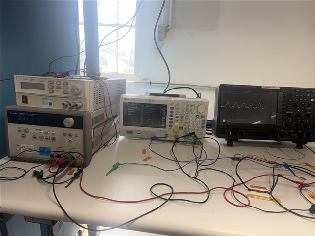
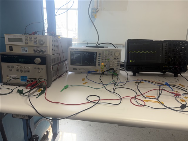
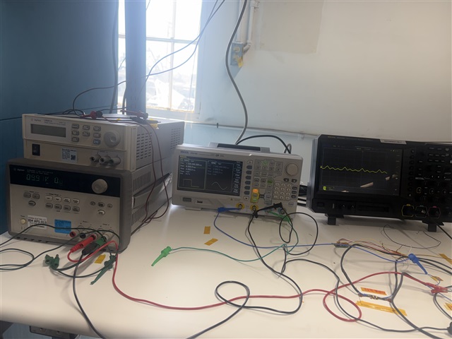
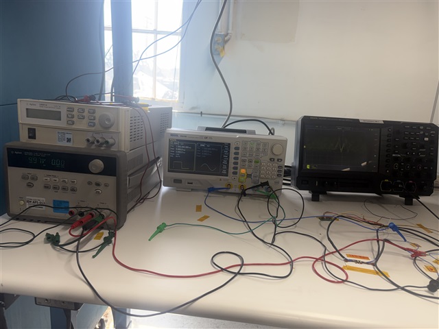
    I have attached for pictures of the setup and results. The test was supposed to be Slew Rate measurement. As you can see from the pictures, I have applied V+=10V and V-=-10V. The circuit is voltage buffer circuit. VIN+ is square wave (from Sig Gen) with amplitudes of 1Vpp, 2Vpp, 3Vpp, 4Vpp. The output was captured on the scope, which is shown in the picture. Let me know if you need more clarification. Thanks

  • Hi Nader,

    Thanks for sending this over. I believe the issue is coming from the fact that this is not done on a PCB from what I can see. In order to get this low of offset measurements using proper PCBs with proper termination makes a huge difference. The issue you could be seeing with the slew rate test is that the long cables are distorting your signals or maybe even reflecting. I would recommend using a proper PCB to collect data on this device as you will likely continue running into issues.

    Best Regards,

    Ignacio

  • Hi Ignacio,

    As I mentioned above, all parameters are bad (VOS, slew rate, swing, everything). Not only slew rate. The slew rate is shown as just a sample. I dont think the issue is with ceramic substate. my OPA2333SHKJ is on ceramic substate and tested under same setup and it works fine. I think the part just went bad. Reliability is important for our application. Any suggestion what went wrong ? Can we send the parts to TI for failure analysis ? AD has AD8634 (flat package), which can withstand 210C, but it is more expensive than TI counterpart. Unit price was the reason we selected TI part . But, we are not willing to compromise reliability and sturdiness with cost. Thanks

  • Hi Nader,

    Is the iq different than what it should be indicating a complete failure? Did you try swapping the failed device with a new device to see if their is a difference in behavior?

    Best Regards,

    Ignacio

  • Hi Ignacio, 

    Sorry, i did not quite catch what iq is ? Could you clarify, please ?

    As I mentioned above, all the parameters are out of datasheet values. Unfortunately, we do not have a second OPA211-HT. As you know, these parts are expensive. We just purchased QTY=1 of OPA211-HT and QTY=1 of OPA2333-HT for evaluation purposes. 

  • Hi Nader, 

    We production test our devices before they are shipped from the factory. They go through extensive validation and final testing. If parts are outside of the specifications listed in the product datasheet table they are discarded in production. Ignacio mentioned the Iq which is the quiescent current of the device. Have you measured the quiescent current of the device in a buffer configuration? If the Iq is not matching the datasheet when configured in a buffer configuration then it is highly likely the device has experienced some form of electrical overstress or ESD damage. 

    Prior to attempting to measure datasheet parameters, a simple buffer test circuit should be used to ensure the device is operating as an op amp. I have included a simulation below. Please measure the Iq shown in the meter below. Also provide an oscilloscope capture showing the input and output 1Vpeak 1kHz input and output for us to analyze. 

    For debugging

    • Please use a buffer configuration to start and measure the quiescent current of the device
    • Make sure the device is operational in a buffer configuration by applying an input signal and measuring the output signal on the output pin. 

    For ESD and EOS

    • Ensure that the devices are being handled in an ESD controlled environment to avoid electrostatic discharge
    • Ensure that the power supply does not have and voltage overshoot that could subject the device to a voltage beyond the absolute maximum voltage in the product datasheet. 
    • Ensure that the input current to the input pins does not exceed 10mA. 

    Best Regards, 
    Chris Featherstone

  • Hi Chris,

    I did per your setup. Rail : +/- 18VDC, Inverting input connected to the output. Non-Inverting input connected to the COM (the middle of +18 VDC and -18 VDC). No output load. IQ started from 11.1 mA and gradually decreased to 10.8 mA (stable), after 15 minutes. Datasheet's IQ is 6 mA (MAX) @ room. My measurement indicates x2, almost. What do you think ? Thanks 

  • Regarding the output waveshape with buffer configuration, please refer to my post (pictures) , posted 5 days ago. Thanks 

  • Please mind you, that in my setup for measuring IQ, IN+ was connected to COM. Whereas, for my post 5 days ago (the setup shown in the pictures), IN+ is connected to square wave 1Vpp. 

  • Hi Nader, 

    To help us provide the fastest support possible, I suggest we consolidate our discussion into one thread. Since the same engineers are monitoring all six open threads, keeping the communication in one place will help maintain continuity and prevent information from being fragmented.

    To move forward with the investigation, could you help us with a few details?

    1. Are you seeing output oscillation when measuring the Iq of 11.1mA?
    2. In the buffer configuration (with IN+ set to COM), what is the DC output voltage?
    3. What is the value of COM?
    4. As a troubleshooting step, have you tried using a general-purpose op-amp to prove out the test setup?

    Best Regards, 
    Chris Featherstone

  • Hi Chris,

    I am not quite clear about your suggestion to consolidate all threads to one.  You mean I have created several threads on OPA211-HT ? If, so, can you go ahead and please consolidate them ? Thanks

    I will measure #1 and #2 (your itemized requests, above) later today. 

    #3 response : COM is exactly the middle of +18V and -18V. 

    #4 response: As I have mentioned in my prior posts, I have used OPA2333-HT in the exact setup, and measurements were very close to datasheet.(VOS, Slew Rate, Input Limit, Output Swing). 

  • Hi Nader, 

    We will await your measurements.

    Best Regards, 

    Chris Featherstone

  • Hi Chris,

    #1. Connecting output to scope, IQ increased to 12.5 mA. Output is shown below in the scope snapshot.

    #2. Output measured by DMM is -0.250 V (-250 mV)

    This is not floor noise. My floor noise is very low, almost thin straight line. Instead, this is coming from OPA211-HT 

    Thanks

  • Hi Nader, 

    The device appears to be unstable within your current test configuration, which is likely caused by parasitic capacitance from the long output cables. This capacitance can destabilize the op-amp, leading to the increased Iq you are observing.

    To demonstrate this, I have included an example below using an extreme case. Note that when the device is unstable, both the Iq and the output voltage show unexpected results. However, by adding a 100 Ω isolation resistor between the output and the cable, the oscillation is eliminated.

    The 11mA Iq measurement you are seeing is likely the average value captured by your DC meter during oscillation. To confirm this is the root cause, please try shortening the output cables or adding a series isolation resistor to decouple the output from the cable's parasitic capacitance.

    Best Regards, 

    Chris Featherstone

  • Good Morning Chris,

    Sure. Let me try that. Thanks. 

  • Hi Chris,

    I connected a 105 Ohms resistor to the output. Measured. Same exact results. The same output waveform, the same output value ( -0.250 V), the same IQ= ~12.5 mA. I think the unit is out of its characteristic parameters. 

  • My output waveform is noisy and hazy, is not clean oscillation as you showed in the diagram in your prior post. 

  • Hi Nader, 

    To help us narrow down the root cause, could you please clarify a few points regarding the test environment?

    • ESD Protection: Is it possible the device was exposed to an ESD event? Additionally, what ESD controls are currently in place for this test setup?
    • Test Methodology: Have you had the opportunity to test the device on a custom PCB with the component soldered?

    Looking at the image provided, the device appears to be mounted to a glass fixture using long wires. This setup introduces significant risks for external errors regarding stability and EMC (Electromagnetic Compatibility) interference, which can be difficult to rule out. We typically recommend a soldered PCB configuration to ensure we are measuring the device's true performance rather than fixture-induced errors.

    Best Regards, 
    Chris Featherstone

  • Hi Chris,

    My OPA211-HT is glued to a white ceramic substrate. There is no external components soldered to this part. I am measuring in the buffer configuration.

    I wear ESD wrist band, while testing, but I cannot rule out ESD damage.

    Most probable cause, though, may be the frequent exposure of the part to the 200C environment. Is this part characterized for a limited time exposure to 200C ? If exposure must be limited, then we should reconsider using this part in our application. 

    As I said before, my other op amp (OPA2333-HT) was used in the exact same setup and the measurements came out all good, only VOS of CH1 is a little off of the datasheet. 

    Would it be possible to send me a free sample to replace this part and to re-evaluate, or I have to buy another one. Thanks

  • Hi Nader,

    In your setup, do you have decoupling capacitors and the other components near the device? It is hard to tell from your image. Regarding the exposure to 200C. This device is rated to operate at these temperatures however the more important consideration is the actual junction temperature of the device and ensuring this is not exceeded. Regarding samples, we do not provide samples for our higher rated devices such as our HT devices. If you are interested in requesting samples of our catalog OPA211, I would follow the link I added below. We would recommend starting with the cheaper catalog device and debug/prove out your test setup like Chris mentioned previously at room temperature. We sell the regular version in high volume and do not have a history of this part being out of spec. We would also recommend implementing this in PCB configuration. 

    https://www.ti.com/ordering-resources/faqs/inventory-product-availability/sample-request.html?srsltid=AfmBOoogdrm4lfcuX24CW-z6hOcn68pRtnnTDj3zcThU4MESt0x4stfe

    Best Regards,

    Ignacio

  • Hi Ignacio,

    Per the evidences I presented in my prior pasts, I strongly believe that the part is no good anymore. Now that TI does not provide replacement, can I ship the part to TI so that TI team perform a failure analysis on the part? I believe that the part might have gone bad because of multiple exposures to 200C. Is there a max time duration the part could withstand 200C ? 

  • The link you posted above, takes me to "Customer Support", then gives me error !! No form !! Also, I tried to find the form for sample request, I was unable to find it on TI. It is so strange !

  • TI site circles me around, without success to find sample request form ! It is highly unacceptable. Can someone help ?