INA333-Q1: Temp sensing using

Part Number: INA333-Q1
Other Parts Discussed in Thread: OPA333-Q1

image.pngIn this schematic My V+ is 5V which is coming from LDO but 5V reference i am using for Vref pin to give resistor divider as attached. that external 5V is generated by reference IC of 5V .Please suggest as LDO is having 5V at output i should generate 5V resistor divider 5V from refernce IC for that offset voltage to always go above ADC ground noise. So i should give from 5V or 5V LDO will also works fine or there will be any drift in measurement issue i will get using LDO vs Reference IC in this case.Please suggest as this Chain is for temperature measurement . image.png

  • Hi Nishant,

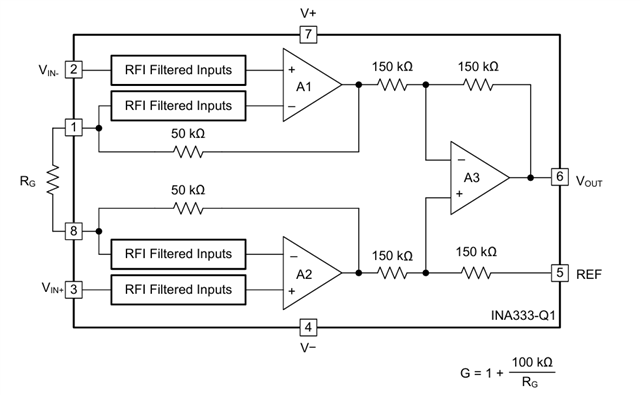
    I'm glad you reached out to clarify this. It's a very common mistake to use a voltage divider using resistors to generate the voltage at Vref. The problem is this will cause many more errors in your system as the resistors will shift the resistor network impedance see on the positive input node of the internal difference amplifier causing a mismatch between the positive and negative inputs as seen below. 

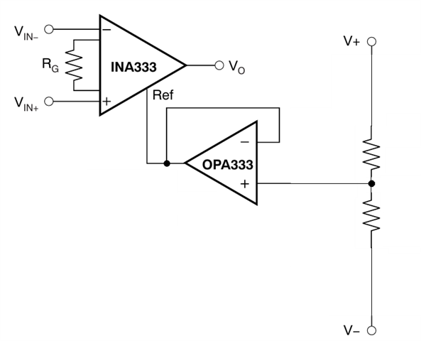
    If you want to use a resistor voltage divider, I recommend putting an op amp in buffer configuration between it and the reference pin of the INA333-Q1 to avoid the impedance shifting the Gain Error and CMRR. 

    Best Regards,

    Robert Clifton

  • So powering Resistor divider with LDO or reference IC which is correct as itbwill taking two IC one Ldo generating 5V and one reference ic generating 5V which to be taken and explain the error in any of these m as buffer i put after that. and what is the best way as you stated OPam as buffer i will put OPA333-q1 between output of resistor divider and reference pin of INA333-q1 

  • Hi Nishant,

    Just to clarify, the reference circuit should look like this: 

    As for the LDO, you do need to be careful. The ESD protection structure consists of ESD diodes on the input going to the supply rails. During any ESD spikes, you will need to have a path to ground from both supply pins. LDOs can rarely handle reverse current conditions, and we recommend including a TVS diode to ground, at the output of the LDO, to give an alternative ground path. 

    Best Regards,

    Robert Clifton 

  • I asked difference between Reference bandgap reference IC of 5V to use for Reference pin as shown in schematic 5V generated by bandgap reference IC which to be put by OPAM buffer then to the references pin . Other option in my mind is 5V supply voltage I am giving using LDO so should I use same Ldo 5V for resistor divider ckt for reference Pin or not . And please tell as I am operating my INA33-Q1 at 5V using LDO I need to add TVS diode ?? If yes which type where bidirectional tvs diode breakdown voltage of ?? 

  • Hi Nishant,

    I asked difference between Reference bandgap reference IC of 5V to use for Reference pin as shown in schematic 5V generated by bandgap reference IC which to be put by OPAM buffer then to the references pin

    I'm sorry I don't understand what you are asking in this sentence. 

    Other option in my mind is 5V supply voltage I am giving using LDO so should I use same Ldo 5V for resistor divider ckt for reference Pin or not .

    Same as the sentence before. Please clarify. 

    And please tell as I am operating my INA33-Q1 at 5V using LDO I need to add TVS diode ?? If yes which type where bidirectional tvs diode breakdown voltage of ?? 

    Technically you don't need it if you can guarantee that the LDO will power up before an input signal is seen on the input pins of the INA333-Q1. Also, you need to guarantee that the input pins do not see a voltage beyond either supply pin. 

    TVS diodes need to be selected such that they remain off during normal powered operation but turn on before the supply pin maximum voltage is exceeded.

    Best Regards,

    Robert Clifton 

  • I have two separate 5 V rails in my design: one supplies the INA333-Q1, and the other is used to generate the REF pin voltage through a precision resistor divider followed by an op amp buffer. Should I use a low-noise LDO or a precision reference IC for the REF pin, while using an LDO for the INA333-Q1 supply? Also, I cannot guarantee that the INA333-Q1 supply will always be available before the input signals. My differential input voltage is always present during measurement and ranges from 0.4 V to 1.2 V, which is well within the valid common-mode range when VCC = 5 V. What happens if the input signals are present while the INA333-Q1 supply is OFF or powers up later? Can this cause back-powering, excessive input current, latch-up, or permanent device damage? If this is not a recommended operating condition, what is the preferred circuit solution to prevent any reliability or circuit failure issues?