OPA2626: Amplifier Settling Time

Part Number: OPA2626
Other Parts Discussed in Thread: THS4551, , TINA-TI

Hello TI Team,

I am designing the analog front end for a 14-bit pipeline ADC. My input signal is a pseudo-digital pulse waveform coming from the source, and it is currently connected directly to the THS4551. The THS4551 is powered from a single supply and converts the single-ended input to a differential output for the ADC.

The signal characteristics are:

  • Input voltage range: 0.2 V to 2.8 V

  • Signal type: Pseudo-digital pulse waveform

  • Rising slew rate: 80 V/µs

  • Falling slew rate: 45 V/µs

  • Output noise from the source: 80 µV

  • THS4551 differential output drives the 14-bit pipeline ADC directly.

I would appreciate your guidance on the following questions:

  1. Is the THS4551 alone sufficient to drive the 14-bit pipeline ADC with this type of pulse input, or would adding an OPA2626 before or after the THS4551 improve settling performance?

  2. What are the deciding factors for selecting an additional high-speed amplifier such as the OPA2626? Is the decision mainly based on the ADC input requirements, the THS4551 settling performance, or the characteristics of the input signal?

  3. How can I calculate whether the THS4551 meets the required settling accuracy for a 14-bit ADC? Which parameters (settling time, bandwidth, slew rate, large-signal response, ADC acquisition time, etc.) should be evaluated?

  4. My input signal is pulse-based rather than sinusoidal. What is the recommended method to verify that the amplifier output has settled sufficiently before the ADC samples the signal?

  5. How can I minimize the effect of parasitic capacitance from the signal source to the ADC input? Are there recommended PCB layout practices or interface circuits that help preserve fast edge rates and settling performance?

  6. My input signal frequency of source is 7.5-10Mhz 
  7. And also tell if i am testing using Function generator analog input SMA connector tehn 50ohm termination is required externally ? if my function generator is 50 ohm impedance state then needed ? .If taking directly from source not function genartor then what terminaion i need to put in my PCB how taht is calculated?

Thank you for your guidance and recommendations.

  • Hello Nishant,

      Thanks for reaching out!

    1. Yes, the THS4551 alone can drive the ADC for a single to differential end conversion for your rise/fall time requirements. Differentially at 2.6V and the THS4551 slew rate, your rise time would be in the tens of nano seconds.  

    2. You would only add a stage before if you
      1. Require more gain while meeting your bandwidth needs
      2. An additional active filter stage
      3. You are expecting input source and FDA to be physically far away (via cabling) and need a buffer. 
      4. If your source has an extremely high output impedance (>10 kΩ) and requires a dedicated high-Z buffer.

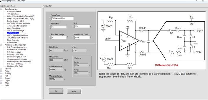
    3. I would recommend watching the video under SAR ADC front-end component selection at this link: https://www.ti.com/video/series/precision-labs/ti-precision-labs-analog-to-digital-converters-adcs.html, and using the analog calculator that we to calculate the necessary RC filter bucket for your settling time to be less than 1LSB. https://www.ti.com/tool/ANALOG-ENGINEER-CALC


    4. For example, in your case, you would need to meet a settling target of  1LSB --> (2.6V)/(2^14) = 159uV, 1/2 LSB --> 80uV. Once you have chosen your ADC, you can check the datasheet for your acquisition time and your capacitance sample and hold value to determine if the system can mathematically settle within the sampling window. Also note that an external RC network is mandatory between the amplifier and the ADC. The external capacitor acts as a local reservoir to absorb the current kickback when the ADC sampling switch closes, while the series resistor isolates the THS4551 to prevent capacitive loading, lowering phase margin which can cause ringing in the transients. In the video linked above, it will show how to use the calculator and then use Tina-TI or PSpice for TI to sweep the RC values and choose the values that will meet your 1/2LSB settling limit. 

    5. Is the THS4551 will be physically located far away from the ADC? The resistor from the RC filter would be enough isolation to the FDA, and then we would recommend the traces to be symmetrically differentially on layout. Also, have the ADC close to the FDA and it's external RC filter. Other layout notes is to have decoupling capacitors at your supplies (small value should be as close as possible to the supply pin of the amplifier, and the larger capacitors can be closer to your power source. We always recommend following the layout shown in the THS4551 EVM, and of course you may remove the baluns at the input and output: https://www.ti.com/lit/ug/slou447/slou447.pdf?. Also, make sure VOCM range of the FDA meets the VREF range of the ADC it is expecting. VREF pin from ADC will be tied to the VOCM pin of the FDA. 

    6. Above takes in account this frequency range.

    7. 7.5-10MHz can be considered needing impedance matching if your traces are long or you are connecting via long cabling. This article has a good explanation on when and why impedance matching is needed. In your case, I would go ahead and still impedance match. Since, you are converting from single-ended to differential, it will be a bit more complicated then just adding 50 ohm to 50ohm since both paths of the FDA must be symmetrical to avoid any common-mode errors at the output. We have a calculator that can help with choosing your RG, RF, and RT (termination) for your application. Link to calculator: https://dev.ti.com/gallery/view/3454860/FDA_Calculator_v3/ver/1.0.0/

    Thank you,
    Sima 

  • Hi TI Team,

    I am designing an analog front end for a fast-changing, pseudo-analog sensor signal and using the THS4551 as the fully differential amplifier/ADC driver.

    I need some guidance on the following architecture:

    Signal source → optional high-speed buffer → THS4551 → differential ADC

    My main requirements are:

    • Fast signal transitions
    • Fast settling with minimum overshoot/ringing
    • Low noise and distortion
    • Adjustable DC offset
    • Differential output with a controlled common-mode voltage
    • Good ADC driving capability

    1. Adjustable DC offset / DC restoration

    I would like to include DC offset adjustment in the initial PCB design so that I can vary the signal's DC level during evaluation without requiring a PCB respin.

    For the THS4551, what is the preferred method to achieve this? As offset voltage is variable not defined currently in design .Offset can vary as per requirement in Real hardware testing that's why asking about one time to do that work and put provision and can change according to the requirement 

    As I told my input specification before you can check and ADC having Vcm of 0.9V for optimal performance and that is tied with Vocm pin with decoupling cap of 1uF 

    Would it be better to:

    • Adjust the VOCM voltage?
    • Inject an adjustable DC voltage into the amplifier input/feedback network?
    • Use an DC coupling + DC restoration approach?
    • Provide resistor/DNP options for future offset adjustment?

    The important requirement is that the offset should be adjustable while maintaining low noise, low distortion, stability, and fast settling.

    2. Buffer before THS4551

    I am also considering placing a high-speed buffer such as OPA2626 before the THS4551:

    Source → OPA2626 → THS4551 → ADC

    Would the additional buffer improve the driving capability and settling performance for a fast-changing signal, or would it generally be better to drive the THS4551 directly?

    Are there any specific concerns regarding:

    • Added settling time
    • Noise accumulation
    • Stability
    • Output impedance
    • Driving the THS4551 input network
    • Overall transient response

    For this type of signal, would you recommend OPA2626 + THS4551, or THS4551 directly from the signal source?

    I would appreciate guidance from anyone who has designed a similar high-speed sensor/ADC front end using the THS4551.

    Thank you.

  • How I can subtract my offset voltage that is coming with My signal voltage. What I can do my Amplifier and ADC Chain to make it do calculate otherwise I will not be able to use my ADC Full dynamic range. My ADC has AVDD=1.8V. 

    This varying voltage is system practical in operation dependent How and what provision I have to put in my circuit to make the signal correctly feed to ADC after subtracting Offset and with attenuation to make it in range of differential 2Vpp also. Please tell what I need to do?

    Amplifier is THS4551 currently only in chain after that ADC. If I need to check my Output voltage waveform before putting in chain? Should I use OPA2626 for checking analog output voltage waveform then header pin connector then with provision of subtracting offset and make the system with low settling time and then use THS4551 and 14-bit high speed pipeline to get good SNR?

    If I use only THS4551 then what provision of Offset need to put and what i can do as signal voltage is 0.2V to 2.8V (pulses) pseudo analog signal as told with slew rate given as mentioned above 

  • Hi TI Team,

    My analog source has:

    • Output resistance: 160 Ω

    • Output noise: 80 µV

    • Maximum load capacitance: 25 pF

    I have multiple analog channels and want to achieve fast settling, low crosstalk between channels, and minimum power consumption.

    What is the recommended approach to:

    1. Minimize the capacitance seen directly by the source output?

    2. Reduce crosstalk between multiple analog channels?

    3. Use a series resistor or buffer without unnecessarily increasing power consumption?

    4. Maintain fast settling how? 

    5. Any recommended termination resistor if any? For floating inputs of Amplifier for this specification of Analog Input for Amplifier as I stated above?

    Any recommended series-R / capacitance range or PCB layout guidelines for this situation would be helpful.

    Thanks.