OPA227: OPA227 constant current source driver circuit

Part Number: OPA227
Other Parts Discussed in Thread: OPA277, OPA192, OPA2192, OPA2156

Hi TI expert

The attachment is the constant current source driver circuit for the OPA227. R4 is the load and is at high side. Now, due to a specific requirement, R4 needs to be connected to ground(low side). How should this constant current source circuit be modified to achieve this?
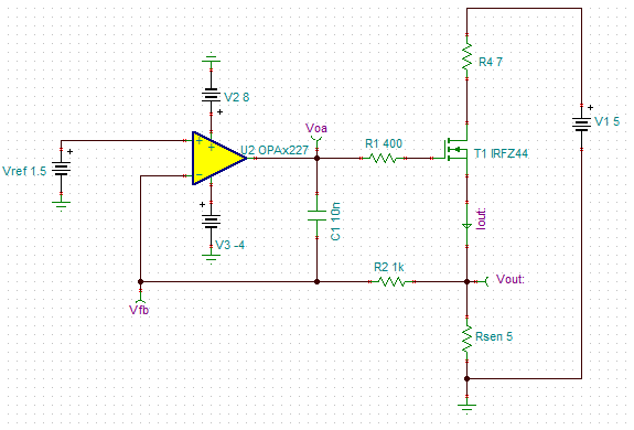
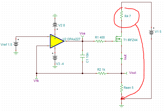
image.png

image.png

Best regards

  • Li,

    You could use the Howland Current Pump with a discrete power transistor output stage.  The simplest solution would only use one transistor, and would only be able to source current.  Let me know if you think this approach would work for you and I can help design the circuit.

    Best regards, Art

  • Hi Art

    I hope you can help me design a Howland current source circuit. Vref is a tunable sine wave, with a minimum of 5MHz, preferably 10MHz.

    Best regards, Li

  • Li,

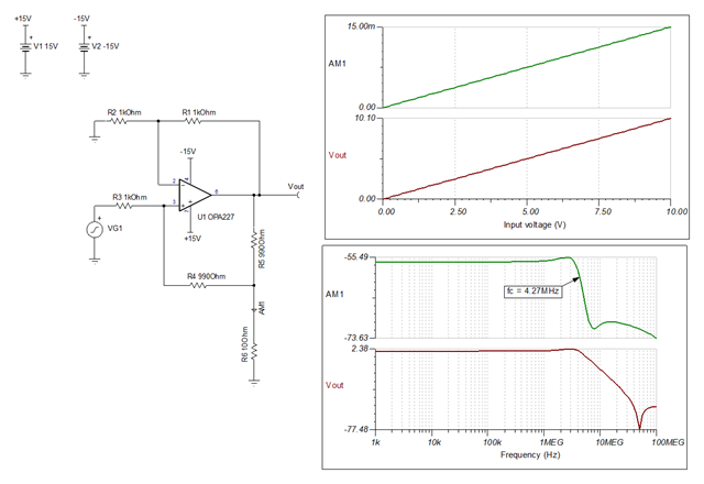
    Below is a Howland current source.  To further refine this design you need to let me know the output current transfer function Iout/Vin.

    holland-current-pump.TSC

    Best regards, Art

  • Hi Art

    The circuit in the attachment has a very small output current. I need the output current to be adjustable from 0 to 0.3A. The input sine wave signal can have a bandwidth up to 5MHz, which means the current signal through the load R6 can also go up to 5MHz. The load R6 is an LED, about 3~5Ω, you can start by simulating with 5Ω.

    Best regards, Li

  • Hello, 

    Art is out of the office today and will return tomorrow. 

    Best Regards, 

    Chris Featherstone

  • Li,

    • Below is a circuit that will output 0mA to 400mA for a 0V to 10V input.
    • You can adjust the function of this circuit using by adjusting R7 and R5.  “Improved” Howland current pump circuit explains the operation of the circuit.
    • The transistor used is a simple NPN power transistor: DXT696BK  . There are many other options that will work.  
    • For the power transistor: make sure you choose R7 to provide enough base current for the function.  Look at hfe (current gain).
    • For the power transistor: make sure you connect the tab to a plane as a heat sink.  Op Amp with Single Discrete Bipolar Transistor Output Drive covers using a power transistor with an op amp.  It is not a holland current pump, but is a high output current op amp circuit.  You will need to confirm that your circuit can handle the required power dissipation.  I selected DXT696 because is has a low thermal resistance, high output current, and good power dissipation capability.  Pay special attention to notes 5,6, and 7 in the DXT696BK data sheet.

    holland-current-pump-with-power-transistor.TSC

    Best regards, Art

  • Hi Art

    Thank you for your reply!

    I still have a question now. I modified your simulation file for VG1, R4, and R5—see the attachment. The input signal for VG1 has been changed to a 1MHz sine wave. R4 was changed to 5Ω because it's used for current sensing. The simulation results show that at an input frequency of 1MHz, Iout < VG1/R5, and the current signal Iout is somewhat attenuated. If VG1's frequency is increased to 5MHz, how should the circuit be modified? Do we need to replace U1 and T1?

    Best regards, Li

    1108.holland-current-pump-with-power-transistor.TSC

  • Li,

    1. I think that there are two issues: 
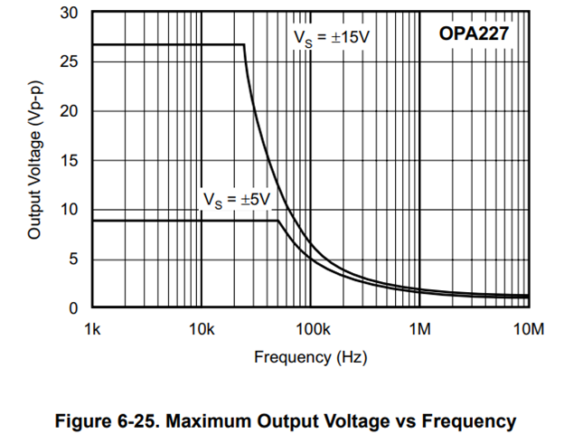
      1. Slew rate limitation. The slew-rate of OPA277 is not high enough for the 1MHz sine wave.  This limitation is also know as full power bandwidth limit or maximum output voltage vs. frequency. Full Power Bandwidth and Op Amp Distortion covers this topic in detail.   Below is the curve for the OPA227.  You can see that at about 20kHz to 40kHz the output swing becomes limited.  You can substitute the OPA227 with an amplifier with higher slew rate.  I did this with OPA192 (similar to OPA227 for DC precision) and the sinusoidal output looks relatively undistorted, but the output is clamped at near zero output voltage.  
      2. The circuit cannot swing to ground.  This is why the output is clamped near GND.  Note that the op amp output will try to push its output high enough to keep the transistor on, but it does not work when Vin is near zero.  I added a 100mV shift on the input signal and the output looks pretty good.  If you want to swing to  Vout = 0V, you will probably need a push pull output (i.e. NPN and PNP).  Hopefully you can accept a small shift in the input signal as this circuit will be much simpler.  

    1108.holland-current-pump-with-power-transistor-opa192.TSC

    Best regards, Art

  • Hi Art

    Thank you for your reply!

  • Happy to help.

    Best regards, Art

  • Hi Art

    “The circuit cannot swing to ground.  This is why the output is clamped near GND.  ”

    I checked the datasheet for the OPA192, and it's rail-to-rail. Is it because of the parameters in the image below?

  • Hi Li, 

    Yes your understanding on the swing to the rail specification is correct. 

    Art wrote a great app note that goes into detail on op amp input and output swing limitations. 

    https://www.ti.com/lit/wp/sboa583/sboa583.pdf?ts=1786399215254&ref_url=https%253A%252F%252Fwww.google.com%252F

    Legacy op amps could only achieve an output swing within 1 to 2V within the power supplies. Modern op amp topologies using CMOS transistors often reach much closer output swings to the rail. This is seen in the table you show in your last response. Note that for a no load condition, the output swing can achieve a typical value of 5mV from each supply rail. This is the reason that modern op amps often use the rail to rail terminology for the output swing; it gets much closer than legacy op amps.  

    Because a MOSFET must always maintain a non-zero VDS to conduct current (when powered and linear), the absolute output voltage is strictly bounded by:
    • Maximum High: +Vs - VDS
    • Minimum Low:   -Vs+VDS

    Where +Vs is the positive power supply and -Vs is the negative power supply. The negative power supply may be GND for a single supply configuration. 

    Visually you can see this below in the diagram. 
    I hope this helps. 

    Best Regards, 
    Chris Featherstone
  • Hi Chris 

    Thank you for your reply!

    Best Regards, 

    Li cunxu

  • Hi Li, 

    No problem, glad to help. Let us know if you have any further questions. 

    Best Regards, 
    Chris Featherstone

  • Hi Art

    Attached is the file I modified based on your simulation file. I added an adder before the Holland circuit and replaced the BJT with an NMOS transistor (SOT-23). VG2 is a 1MHz sine wave. From the simulation results, Iout = VG1/R5. 

    The diagram below is a schematic designed based on the simulation file. In actual testing, the output of the signal generator was set to the sine wave corresponding to the simulation file and fed into the circuit through the SMA connector. The test results showed that when the sine wave was 100 kHz, the voltage of load R770 was normal, and the current was also normal. When the sine wave was 1 MHz, the voltage of R770 was half of what it was at 100 kHz, which means the current through load R770 was reduced by half.

    Why do the actual test results not match the simulation?

    opa192 holland-current-pump+power-transistor.TSC

    Best regards, Li

  • Li,

    1. Glad to see that you are close to a working solution!
    2. If you simulate the bandwidth, you get about 2.1MHz.  This means at 2.1MHz the gain (output signal) will decrease by 0.707 of the value at lower frequencies.  This does not match what you see in the lab, but it does show that you are near the circuits bandwidth limit.  Keep in mind that there will be some variation in your component values (resistors capacitors and op amp).  
    3. I replaced the OPA2192 with OPA2156.  This have roughly 2x the bandwidth.  I also replaced the 200 ohm feedback resistors with 2k and dropped the feedback cap to 10pF.  The new circuit has a bandwidth of 5.8MHz.  
      1. The 200 ohm feedback is too small.  These resistors act as a load to the previous stage.
      2. You may want an even higher bandwidth op amp.  You really don't want to expect a flat bandwidth near the bandwidth limit of the op amp.

    holland-wider-bw.TSC

    Best regards, Art

  • Hi Art

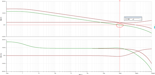
    Is the bandwidth simulation the same as the loop stability simulation, as shown in the attachment? The attachment is your reply when I asked you questions before. 

    0216.opa192 howland+mos-filtered.TSC

    Is the frequency in the red circle in the picture the bandwidth?

  • Li,

    Yes.  The point where loop gain goes to zero or Aol intersects 1/Beta is the bandwidth as well as the point where stability is tested.  The fact that 1/Beta is at 20dB is why the bandwidth is limited to lower than the gain-bandwidth of the OPA192.  I took your plot and adjusted the axes scailing to emphasize that 1/Beta is at 20dB.

    Best regards, Art

  • Hi Art

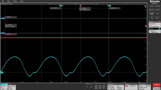
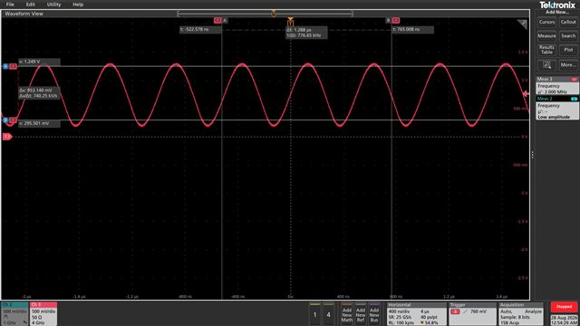
    This week I bought some OPA2156 to replace the OPA192. The test results are shown in the picture. The input signal works fine at 2MHz with no attenuation. But there's a bit of distortion for signals around 1MHz. Can you tell me what might be causing this and what changes I need to make?

  • Li,

    Usually when you get distortion at high frequency this is from slew-rate limitations.  However, this distortion generally converts a sinusoidal waveform into something that looks like a triangle wave.  Your distortion looks a little different than what I would normally expect for slew induced distortion, but I think we should still consider this as a possibility.  Slew induced distortion is amplitude dependent.  That is if you see the distortion at a particular frequency (e.g. 1MHz), the distortion should be worse for larger amplitude signals and better for smaller amplitude signals.  If you reduce the amplitude of your output signal does the distortion reduce?  If it does you need an amplifier with higher slew rate. You may need to move to a "high speed" amp.  We call amplifiers "high-speed" that have bandwidth of 50MHz and higher.

    Best regards, Art

  • Hi Art

    I repeated the test a few more times, and the 1MHz distortion didn’t show up. It’s possible that back then, environmental factors coupled noise into the oscilloscope or the signal being tested.

    Best regards, Cunxu

  • Cunxu,  

    Good news.  Best wishes on your continued success with your project.  Let me know if you have other questions.

    Best regards, Art