Part Number: OPA892
Other Parts Discussed in Thread: TLV3901, TLV3811, TLV3801
Hello TI Engineer,
We have a project that requires a clock waveform conversion circuit, with the following specifications:
-
Input frequency: 100 MHz
-
Signal waveform: sine wave
-
Input level: 3 dBm to 5 dBm
-
Input DC offset: < ±50 mV
-
Output impedance: 50 R
Here's my initial approach:
-
Since this is a 100 MHz clock and we need to preserve the higher-order harmonics, a high-speed op amp or comparator is required. I'm considering a device with a bandwidth greater than 1 GHz.
-
The output needs to be a 3.3 V LVCMOS square wave to interface with a CPLD, so I plan to use a comparator to convert the sine wave into a square wave.
-
From my calculations, 3 to 5 dBm into a 50 R coaxial cable gives a voltage swing of roughly 1.3 V.
-
Because there may be a DC offset up to ±50 mV, I intend to use AC coupling to remove it.
My proposed implementation:
-
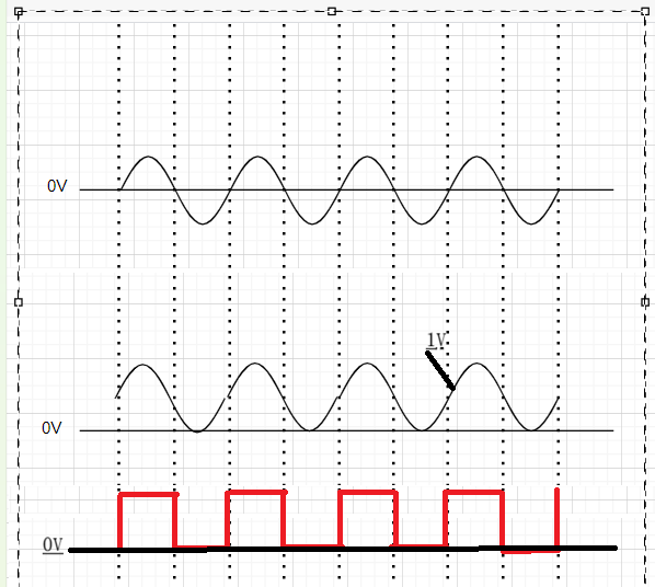
At position 1 in the diagram, place a capacitor for AC coupling to strip off any DC offset.
-
At position 2, apply a DC bias to eliminate the negative portion of the sine wave (please refer to the two sine waveforms in the drawing).
-
At position 3, set a comparator threshold voltage using a resistive divider. However, since the input amplitude varies between 3 dBm and 5 dBm, a fixed threshold (I used 1 V) causes the output duty cycle to deviate from 50%.
Note: The intended behavior is that when the input voltage is above 1 V, the output goes high, and when it's below 1 V, the output goes low.
Could you please review this approach and let me know if it's feasible, or if there's a better solution you would recommend? If a comparator-based design is the way to go, what aspects could be optimized? Thank you.