INA4230: INA4230 accuracy issue - setting adjustment suggestions

Part Number: INA4230
Other Parts Discussed in Thread: CS-AMPLIFIER-ERROR-TOOL

hi sir,

Currently, in our validation, the INA4230 power error is higher than 1.5% of the datasheet.

It seems to be related incorrect settings.

Please provide adjustment suggestions to us to improve accuracy, thanks.

  • Hi Zeer,

    You could try maximizing the conversion times and averaging settings, along with that, please refer to the following FAQ: [FAQ] INA228: Current not reading as expected 

    Best,
    Mallika Senthil

  • Hi Mallika,

    You could try maximizing the conversion times and averaging settings -> I'm not quite sure what "maximizing" means. Does it mean fastest conversion time? Highest number of attempts for average.
    Kindly support us below, please,
    Do you have any more specific suggestions, please?
    Are there any examples of golden settings could provide to us for reference?

    And, please you also please review our settings below to see if any adjustments are needed? thanks.
    Current Setting
    Item
      CH3-C2C
    Shunt Resistor Value 3.052 mΩ
    ADC Range (ADCRANGE) 0
    SHUNT_CAL Register 4193
    Averaging Mode 1024
    Conversion Time 1100 µs
    Current_LSB Setting 0.000400 A/bit
    Regards,
    zeer
  • Hi Mallika,

    we have more experiment, but not improved.
    Before develops INA4230, we have to calibrate if good enough to use. Our experiment is correlation between equipment DAQ and INA4230.
    The measurement is at the same time to record power on DAQ and INA4230.

    The setting I posted yesterday, we have -5.7% variation after tested (power measured by INA4230 is lower).

    We tried below setting, we got -18.2% variation. (not improve).

    Item

    CH3-C2C

    Shunt Resistor Value

    3.000 mΩ

    ADC Range

    0

    SHUNT_CAL Register

    4267

    Averaging Mode

    1

    Conversion Time(VBUSCT)

    1100µs

    Conversion Time(VSHCT)

    140µs

    Current_LSB Setting

     0.000400 A/bit

    Data Readout Method

    ENERGY Reg


    We tried below setting, we got -18.8% variation. (not improve).

    Item

    CH3-C2C

    Shunt Resistor Value

    3.000 mΩ

    ADC Range

    0

    SHUNT_CAL Register

    4267

    Averaging Mode

    1

    Conversion Time(VBUSCT)

    140µs

    Conversion Time(VSHCT)

    140µs

    Current_LSB Setting

     0.000400 A/bit

    Data Readout Method

    ENERGY Reg

    Based on this approach focuses on we do not observe the improvement delta.
    Please kindly support us, thanks.

    Regard
    zeer

  • Hi Zeer,

    Apologize for the confusion, when I said maximize the conversion times and averaging settings, I meant set conversion time to the longest (8244µs) and averaging to largest (1024). 

    Your current register settings seem correct, however, with a current_LSB of 0.0004, you are only utilizing half of the ADC range (80mV), this could add to the error we are seeing. Along with this, the INA4230 measures bus voltage at the IN- pin, check if your DAQ is measuring power after the shunt resistor or before it. Note, as mentioned in the FAQ linked above, the device and system must share the same ground and layout is important to minimize errors. Please share your schematic, layout and maximum current measured in your system. 

    Best,
    Mallika Senthil

  • hi Mallika,

    Could you let us know which register we provided is correct?

    The measured Rsense between DAQ and INA4230 is the same one.

    Some condition:

    It is common GND already.
    Estimated max current is 10A.
    Rsense is 3mOhm.
    The estimated max is 30mV. That’s why we configure ADC range to 80mV.
    The variation is still not improved if DAQ bus voltage is at the IN- pin (load side) and IN+ pin (source side).

    Below are sch and layout for INA4230.

    Left side is power IC.

    Here is INA4230


    Here is routing.
    The center U403 is INA4230.


    Please help us with the problem we are currently encountering.

    Another question:
    Regarding power monitoring accuracy:
    – 1.5% full scale (maximum).
    Does this mean the error is within 1.5% only at full scale (maximum 20mV or 80mV)? Is there a curve description for what happens if the voltage is less than the maximum? could you share to us, please? thanks.

    thanks.

    regards,
    zeer

  • Hi Zeer,

    I'm looking into this, I will get back to you on Monday.

    Best,
    Mallika Senthil

  • hi mallika,

    kindly provide you suggestions, please? thanks.

    regard,
    zeer

  • Hi Zeer,

    Apologize for the delay in my response. The power monitoring accuracy (1.5%) is for full scale differential of 81.92mV and a bus voltage of 48V. Looking at your schematic (which I don't see any issues with), you appear to be using 0.78V bus voltage, which is a very small fraction of the full bus voltage, this is probably where the bulk of your error is coming from.

    As for register settings, what you have currently is fine, but for a slightly better result you could set conversion time to the longest (8244µs) and averaging to largest (1024). 

    Best,
    Mallika Senthil

  • hi mallika,

    Could you explain more, please?

    "you appear to be using 0.78V bus voltage, which is a very small fraction of the full bus voltage, this is probably where the bulk of your error is coming from."

    Not sure why impact between INA input common mode bus voltage and voltage on Rshunt?
    As our Knowledge, ADC range defines measurement accuracy already, please.

    Another question:
    Regarding power monitoring accuracy:
    – 1.5% full scale (maximum).
    Is there a curve to show if the Rshunt voltage is less than the maximum? could you share to us, please? thanks.

  • Hi Zeer,

    The power total measurement error (PTME) is defined as sum of Bus voltage gain error (GBERR) and Shunt voltage gain error (GSERR), i.e. PTME = 0.75% + 0.75% = 1.5%, at full scale voltage (48V) and current.

    So the PTME is composed of two different errors, one from bus measurement and the other from shunt measurement. My earlier comment "you appear to be using 0.78V bus voltage, which is a very small fraction of the full bus voltage, this is probably where the bulk of your error is coming from" hypothesizes that most of the PTME error is coming from bus voltage measurement.

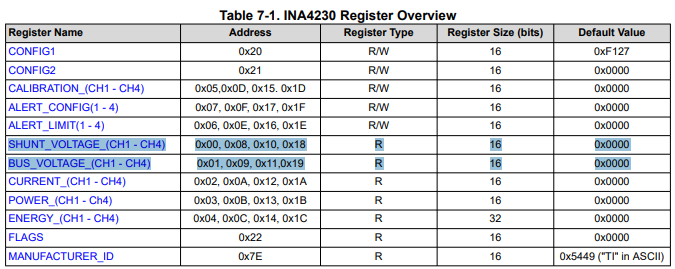
    You can check this by reading from the shunt_voltage and bus_voltage registers and calculating their individual errors to see which one dominates.

    Unfortunately we don't have a curve to error over shunt voltage, however, we do have the error calculator tool [www.ti.com/.../CS-AMPLIFIER-ERROR-TOOL], which we can use to find total error% over current.


    Best,
    Mallika Senthil


  • hi millika,

    we will have more experiment to validate, and will consult to you later.

    please you share again, link is not complete, thanks

  • Hi Zeer,

    Here is the complete link: https://www.ti.com/tool/CS-AMPLIFIER-ERROR-TOOL

    Best,
    Mallika Senthil

  • hi mallika,

    we validated different power rail with VSYS (it is 20V) by DMM and INA. It has quite difference, and should be something wrong.

    DMM: 6.5W.
    INA: 27W.

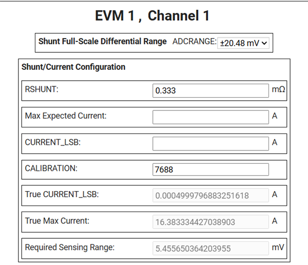
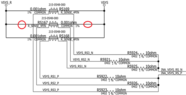
    Below is design and setting. could you review again and give us suggestions, please, thanks.

  • Hi Zeer,

    1. What is the correct expected power measurement?

    2. Where did you probe using the DMM? Please probe the points circled in red.

    3. What is the max expected current you used for calculations? Was it ~16.3833A?

    Your schematic looks good, the filtering capacitor of 10uF is a little too large, perhaps a 0.1uF may be better, but this is not the likely cause for the error we're seeing.

    I'd like to check the layout as well, please share. One more thing to review in terms of layout, since you have 3 shunts in parallel, layout is critical to ensure that the current is split equally. Please see the following app note: https://www.ti.com/lit/an/sdaa115/sdaa115.pdf

    Best,
    Mallika Senthil

  • hi mallika,

    1. we expect INA could be align with DMM in VSYS case, and is within 5%.
    3. max expected current ~16.5A with voltage=20V.

        Currently, the measurement power is ~6.85W in DMM.
        DMM measurement is ~ 0.113mV. 113/0.33mOhm~0.37A -> 0.37A*20V=6.85W.

    2. i'm not sure why can't attached picture here. i will attached measurement point and layout picture later, please, thanks.

  • hi mallika,

    could you share you mail, too, please?
    i can't attached picture, it is seems website maintainess. i will send picture to you by email.
    in future i will still post issue by forum, please, thanks.

  • hi mallika,

    the measurement point is here,

    below is layout.

    Please give your suggestions, thanks

    if possible, please share your email address, i could send picture, please, thanks.

    Regards,
    zeer

  • Hi Zeer,

    Thank you for your patience. Layout and schematic all look fine, where you're probing with the DMM is also fine, but I would check that the DMM has enough resolution to measure 113uV.

    Please provide a complete register readout, I want to check if the current and voltage measured by the device are correct. Power is calculated off these measurements, so next step is to check whether the issue is in the current or voltage measurement.

    Also, please note, you have set max current to 16.5A, but you are measuring 0.37A. This is a very small value in the range you've set. Also the device offset is ~75uV. So if your DMM is measuring 113uV, then the device's offset will add 75uV (max) to this and INA4230 will measure 188uV across shunt.

    I will send you a private message with the team's email id on e2e.

    Best,
    Mallika Senthil