OPA2994: Schematic Review

Part Number: OPA2994
Other Parts Discussed in Thread: ADS7138

Hello Amplifers Team,

I'm an applications engineer from DLP team developing an EVM featuring your device, OPA2994. I'm using each to buffer a DAC output channel, may need to drive a 20 kHz signal. Using dual feedback to improve transient settle time. Please let me know if you have any suggestions to improve the schematic.

Schematic - p67 PLM EVM - DLP135.pdf 
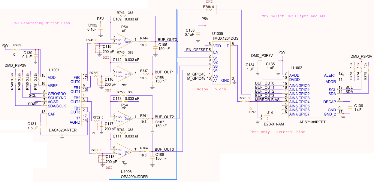
image.png

  • Hello, 

    We will need 1 business day to respond. Thank you for your patience. 

    Best Regards, 
    Chris Featherstone

  • Please also let me know the device operating quiescent current frequency so I can further optimize Cin. Thanks!

  • Tilden,

    1. The main reason for using the dual-feedback method is to stabilize an op amp circuit for capacitive drive, and also be able to drive a varying DC load impedance.  The circuit is discussed in detail in Operational Amplifier Stability Theory and Compensation .   
    2. Another approach that compensates op amps so that they are stable is the Riso method.  The Riso method has the disadvantage of not being able to drive a varying DC load.  However, in your circuit there is no DC load (IDC = 0A).  Thus, the dual feedback approach is not needed.  Your circuit does not have a DC load because you are driving the input of a SAR ADC.  The input of a SAR ADC is the sample-and-hold circuit.  This circuit is just and RC circuit and does not draw any current after the sample capacitor is fully charged.  The Riso circuit has faster settling than the dual feedback approach.
    3. The op amp you selected has "unlimited capacitance drive".  This means that it should be stable to drive 150nF  without additional compensation.  Although it is stable for capacitive loads, the phase margin does drop to 20deg for a 150nF load (see figure 5-40).  I do think using an isolation resistor is a good idea to improve that phase margin, minimize the overshoot, and improve settling time.  However, I do not think that using the dual feedback method is necessary or helpful.  It makes your settling time worse than the Riso method.  Below is the simulation of your circuit and the simple Rios version of your circuit.  You can see much better settling (and a less complex implementation) for the Riso circuit.
    4. Regarding your question "let me know the device operating quiescent current frequency so I can further optimize Cin".  Quiescent current is the DC power supply current when the circuit is unloaded without a signal applied (Vin = 0V).  I am not sure how to help with this question.  The capacitance is normally selected to provide a charge reservoir for the SAR ADC.  This value is adjusted for optimization based on the ADC requirements.  Normally, the value is most critical for high resolution and high speed applications.  Your resolution is quite low (12 bits).  Also, the maximum sampling rate of ADS7138 is pretty low, so the capacitance value is not critical.  Generally for many SAR ADC, the minimum capacitance is about 1nF.  Using larger input capacitance will reduce the settling time, but otherwise is not an issue.  The settling time is reduced because the capacitor needs to be charged up (RC time constant).   You could probably reduce your input capacitor to a much lower value to reduce settling time but I don't think it really matters much because your sampling rate is low and you don't really need very fast settling.

    Best regards, Art

  • Hi Art,

    The man himself.

    Thanks for your reply, I didn't realize this was your team. I actually read through the first half of your white paper quite in-depth while working on this portion of my design - very educational and interesting, I enjoyed learning from it. Still need to go through the 2nd half.

    I should have clarified this earlier - my schematic does not show the entire circuit. The MIRROR-BIAS net on ADC pin 3 is actually connected to my team's DLP device, it has a capacitive load, possibly resistive too (I'm unsure since they are still building it). I implemented dual feedback to be as accomodating as possible. If there is no resistive load, I figured I could just implement regular unity-gain feedback by replacing CF with 0-ohm resistor and removing RF. I wasn't sure if the parasitics of a 0-ohm would have any significant impact on the feedback loop vs. direct trace, let me know if you have any thoughts here.

    Please also let me know the device operating quiescent current frequency so I can further optimize Cin

    Sorry for any confusion here, I am referring to the op-amp's Iq. I see in the op-amp d/s 1.35 mA per amplifier. Since Iq is typically given as DC value I was wondering if the device actually PWMs drawing a larger amount of current at a given frequency so I could optimize the decoupling capacitor for this frequency.

  • Tilden,

    1. Thanks for your kind words.  I agree with your plan to implement the dual feedback given that you may drive a resistive load.  I also agree that it you end up not having the resistive load you can just populate the circuit using the standard Riso. 
    2. Regarding the power supply current.  You are correct that the power supply current will increase due to the PWM signal.  SAR ADC Power Scaling covers how digital current increases due to driving a square wave onto the parasitic capacitance of a PCB trace.  Althought that is not exactly what you are doing, the theory is the same.  Basically current is given by the relationship Isup = C x (VpwmMax - VpwmMin) x fpwm.  This is based on the relationship I = dQ/dt, and Q = C x V.  The PWM current will add to the op amp quiescent current to give you the total power supply current. 

    I hope that helps, Best regards, Art