This thread has been locked.

If you have a related question, please click the "Ask a related question" button in the top right corner. The newly created question will be automatically linked to this question.

Photodiode AC Amplifier

Other Parts Discussed in Thread: LMH6601, LMP7717, OPA356, OPA365, OPA37, OPA132, OPA140

Hi,

I want to build a photodiode amplifier to get an AC signal at a frequency of 1 Mhz.

My photodiode has a parasitic capacitance of about 4pF.

I want my system to work in a dark room or with sun light beams on the photodiode. => The photocurrent would vary from about 0.1µA to 70µA. The AC signal will be about 0.3µA.

I tried to simulate different topologies (transimpedance amplifier, etc) without any good results.

It seems that I don't succeed to remove the DC component properly...

Any help will be appreciated !

Different topics I read:

http://e2e.ti.com/support/amplifiers/precision_amplifiers/f/14/t/167369.aspx

http://e2e.ti.com/support/amplifiers/precision_amplifiers/f/14/t/96946.aspx

Thank you !

  • Vianney,

    Are you detecting the signal from an LED or laser? The first and easiest step in improving the ratio of AC signal to DC background light may come from optical filtering. A narrow wavelength filter can greatly reduce the background signal level.

    The first link you provided in your message shows two possible two-op amp approaches. The first uses relatively low transimpedance gain to accommodate the high ambient light signal, AC-coupled into a second amplifier. The second approach uses a feedback op amp and transistor to counteract the ambient light level.

    Can you provide some details on the circuits you have tried? This would give us some background on the op amp selections and power supply arrangements you have tried. We also might possibly spot simple problems that you have overlooked.

    Regards, Bruce.

  • Hi Bruce,

    Thanks for your answer.

    The source signal il an IR LED. I plan to have IR filters and my photodiode has already an embedded filter :). I would like to have only a +5V power supply and if possible tiny packages like SC70 (prefered) or SOT-23 amplifiers.

    More precision about my needs.

    I have 8 photodiodes and a multiplexer. The final goal is to have this configuration:

    Photodiode 1    |
    Photodiode 2    |
    ...                       | MUX -> Amplifier -> Trigger -> µC
    Photodiode 7    |
    Photodiode 8    |

    I have one topology which seems to work in simulation: http://www.kirikoo.net/images/7force-pc2-2-20120415-221355.png
    It's a simple voltage follower -> multiplexer -> voltage amplifier. I can add a band pass filter centered on 1Mhz before or after the final amplifier.
    What do you think of thas topology ?

    I tried to pu the multiplexer just after the photodiode but with no result. It seems all the photocurrent goes into the multiplexer parasitic capacitance...
    The schematic: http://www.kirikoo.net/images/7force-pc2-3-20120415-221355.png

    Finally, with a transimpedance amplifier, I have to put a low gain for my system to work with sunlight (feedback resistor of about 15k-20k). Moreover, the feedback capacitor (for stability), generally founded on transimpedance configuration has to be very small for the system to work at 1Mhz. It's a problem to have capacitance of about 1p - 2pF...

    I didn't found an efficient manner to compensate the effect of sun. I understand that it's better to have a transimpedance amplifier with a high gain but how to remove this DC component? That's the question :).

    Regards,

    Vianney

  • Vianney,

    Your two circuits operate the photodiode in photovoltaic mode which is requires that the load resistance be pretty low to achieve the desired frequency response. And, as you have seen, the additional capacitance of the multiplexer ahead of the first op amp makes this approach far too slow.

    Does your first circuit appear to operate properly? It appears that the AC coupling should remove the ambient light signal. Is this where you are having a problem?

    Regards, Bruce.

  • Hi Bruce,

    Yes my first circuit seems working in simulation. I have to prototype it. The only drawback with it is the need of a voltage follower after each photodiode.

    I have to deal with a very small space on my PCB, a solution with the MUX directly after the photodiodes would be welcomed.

    I have a transimpedance amplifier which works in simulation: http://www.kirikoo.net/images/7force-pc2-20120416-191114.png
    Different points with this schematic:
    + The MUX can be put just after the photodiodes
    -  "Low gain" due to the high DC component (about 6mV pk pk in output).
    - "Little" bypass capacitor which could be hard to achieve.

    Do you see a way to have a better design ?

    Thank you.

    Vianney.

  • Vianney,

    I'm not sure you have simulated the multiplexing function. Keep in mind that the high-pass filter function that removes the ambient light level must stabilize to a new DC value when you switch channels. This will limit the speed at which you can scan the channels.

    Any attempt to multiplex at the input of a transimpedance amp (TIA) is greatly hindered by the large multiplexer capacitance (approximately 100pF). You may be able to improve this with selection of a multiplexer with lower capacitance. In any case, it takes a wide bandwidth op amp to deal with this issue. With the combination of lower capacitance and a wideband op amp you might succeed with a TIA approach.

    You have not commented on my suggestion of a two-op-amp loop for elimination of the ambient light level. This would allow use of a much larger feedback resistor in a TIA without overload. The current in T1 stabilizes to a value that balances the photodiode current due to ambient light. This does not, however, solve the problem of multiplexer capacitance. I've shown the schematic for this two-op-amp loop below for your consideration. This version is not designed for single supply operation and is just shown as an example of the approach.

    Regards, Bruce.

  • Hi Bruce,

    Yes I noticed that the coupling capacitor will introduce a delay for the signal stabilization around the bias point of the op. amp.

    I will look for some better multiplexers. By "wide bandwidth" you mean Gbpw / A >> 2Mhz ?

    About your approach, I have some difficulties to make it working. What can you advise me to adjust it?

    My first approach would be to adjust R1 and C3 to have a good gain + stability with no DC component. I'm not sure to understand the role of the integrator...

    Thank you !

    Best regards.

  • Vianney,

    I should have provided a schematic that more closely resembled your situation. I've attached a new one with some annotations that may help.

    R1 in this diagram could be set to 300k or so. With 0.5pF stray capacitance on R1, bandwidth would be limited to somewhat over 1MHz.  Your ambient light signal of 70uA would create too much voltage on R1. R2/C1/U2 integrates the output voltage, compared with Vref (2.5V). It drives current source T1 to create a balancing current equal to the 70uA ambient light current. Thus, the net average DC current in R1 will be zero. This loop will hold Vout at an average voltage of 2.5V, even if the ambient light level varies.

    This approach allow use of the highest possible transimpedance gain, R1 without overload from ambient light. The gain-bandwidth requirements of the circuit depends on the ratio of the impedance at the summing junction to the impedance of the feedback network. With 100pF at the summing junction and less than 1pF on the feedback, the circuit requires an op amp with hundreds of MHz GBWP to achieve 1MHz signal bandwidth. If you can get the capacitance at the summing junction much lower, you may have a chance of multiplexing the input.

    Regards, Bruce.

  • Hi Bruce,

    Thank you for your schematic, it works great in simulation. I had to decrease R1 to about 330k but it's ok.

    Moreover, I found a better multiplexer, a TI one, with 24pF input capacitance, 75ohms on resistance and 6pF out put capacitance. Multiplexing the anode of the photodiode seems to give good results. I have to prototype it now.

    About the choice of the op. amp I think the LMH6601 or LMP7717 are good choice for the transimpedance amplifier, any suggestions on that ?

    Regards,

    Vianney

  • Vianney,

    I have no personal experience with the LMH6601 or LMP7717 as I support the "OPA" branded products. Upon quick look, they look like reasonable possible selections. You may also want to look at OPA356 and OPA365 which resemble these "LM" products in some respects. Final choice could depend on factors I'm not delving into. I suggest some careful simulations with your choice to help optimize the circuit.

    Regards, Bruce.

  • Hello Bruce,

    I have implemented your design idea into my photodiode application.  My question is what is the purpose of the T1 and U2?   Does it tottaly blocks the ambient light?  I tryinging to detect modulated green led from the unit. and display the serial data on hyper terminal.  Thank you for your help.

    Regards,

    Amit


    8875.SCH_21009362_REV-B (2).pdf

  • Amit,

    The purpose of T1 and U2 is to create an equivalent response of AC coupling of the photodiode. Conventional AC coupling with a series capacitor is not possible at the input of a photodiode transimpedance circuit as it would allow the photodiode to become forward biased. T1 and U2 form an integrator feedback loop, sometimes called a DC servo correction, and drives the average DC output of U1 to the voltage applied to U2's non-inverting input.

    Regards, Bruce.

  • Bruce,

    Thank you for explanation.  What should do to remove ambient light from Fluorescent, lamp, incadescent lamp etc..?  I have a high pass filter after transimpedence amplifier.  Is that enough?

    thanks

    Amit

  • Amit,

    The circuit values I showed in an earlier posting on this thread would provide good attenuation of background light signals up to several hundred Hz. Additional filtering on the output as you have done would also help. If you need assistance to optimize your application, I suggest that you start a new thread posting so that your requirements are not confused with this thread.

    Regards, Bruce

  • Hi,

    I am building a circuit that needs to amplify the AC light signal and reject the DC part in a similar way to the topic here. I need  1 M Ohm amplification and a bandwidth more than 1 MHz. I already built the circuit and the Trans-impedance amplifier (TIA) is working fine as required. The DC restoration circuit is also working but it is generating high frequency oscillations around 25 MHz with an amplitude of 200 mV. The oscillations are periodic. The simulation shows no problems.

    I used a circuit similar to this one .. (The TIA part i used consist of 2 opamps to increase the bandwidth)

    I took the DC restoration circuit from a design by one TI engineers (Bonnie Baker)

    http://www.edn.com/file/25838-Photosensing_with_ambient_background_PDF.pdf?force=true

    To solve the problem i tried to add a resistor in parallel to C8. I also tried to reduce/increase R6... No effect was seen. I also tried exchanging the opamp (OP37) with OP847 but this time it did not work at all. Just went into saturation.

    I hope to get some hints to solve the problem. I feel that the DC restoration OpAmp is instable.

    Thanks

  • Samer,

    The OPA37 is not unity-gain stable and thus cannot be used as an integrator. C8 provides a low impedance at high frequency and effectively puts the op amp in unity gain which can cause the op amp to oscillate.

    OPA132 or OPA140 are possible replacements.

    Regards, Bruce.

  • Thanks Bruce for your fast response. I missed this fact. I will try with the opamps you recommended.

    By the way, which method you think is better. The one i used or the one you described above? I think that the method using the transistor to compensate the current could provide a wider operating range. But i was not sure if it gives more noise.

    Regards, Samer

  • Hi Samer,

    I have not thought too much about which circuit technique might be better. I made my design (using the transistor) in response to a question on the forum. This forum question was after Bonnie published her note, though I had never saw or read it. Had I known of her note, I might have just referred to it.

    I agree that my method may allow wider range control of ambient light, especially if the degeneration (emitter resistor) is reduced. I suspect that Bonnie's circuit will achieve lower capacitance at the summing junction, a possible advantage if your photodiode capacitance is quite low and wide bandwidth is required. My transistor circuit creates a much higher impedance current source on the summing junction at low frequency. This may have an advantage in some applications.

    Regards, Bruce.

  • Hello Bruce,

    Could you please explain what is purpose of T1? what it does? How does it do it?  Wouldn't it make Vout to oscillate or Photo diode?  I guess i don't understand properly the role of U2 and T1.

    Thank You,

    Amit Pael

  • Amit,

    Sorry to ask for this but could you please resubmit your question on a separate thread (start with a new question). This thread refers to another thread that has the schematic that you are referring to. It also has several other schematics so it has become very confusing. The resulting discussions have been very hard for others to follow. I suggest the following title to the post:

    AC-coupled photodiode amplifier to reject ambient light

    Thanks and regards, Bruce.

  • HI Bruce, I have been analyzing this circuit and it seems like a very good way to remove ambient light. I have been simulating this and have been running into some stability problems (simulating with an "ideal op amp") at higher ambient currents >32 uA.

    Can you comment on the stability criteria for this circuit and what magnitudes of DC current it can reject?  Why  does this design use an integrator rather than a standard low pass?

    Also, what kind of noise does this method of DC servoing introduce?

    Thanks for you help,

    Chris

  • Hi Chris,

    I'll reply to your other posting relating to this question. See it at...

    http://e2e.ti.com/support/amplifiers/precision_amplifiers/f/14/t/300533.aspx

    For all who may read this:  Be aware that new questions added to the end of a long thread such as this one are often overlooked or ignored. It's best to post a new question on a new thread as it is much more likely to get attention.

    Regards,  Bruce.

  • Hello Bruce,

    thanks for your suggestion. In my application (vibration recording via reflex coupler 10Hz..10kHz) I have single supply only. It seems that I found a simple solution that will do the job. I report (very late after your contribution) so that someone can participate as I did/do here...

    Andreas

  • Amit,

    It is nice to see that you are designing a photo sensing circuit. This is the type of design that I have been involved with for years. I just saw you conversation with Bruce and there are some thoughts that come to mind.

    In reference to your attached circuit.

    • U1-D performs your I-V conversion. With this circuit the transimpedance gain is 2 MA/V. For your ac signal you will get a theoretical peak to peak signal of 0.6 V centered around 1/2 Vdd.
    • The U1-D signal bandwidth ~ 7.96 kHz. In your previous discussion I was of the impression that you wanted a signal bandwidth of ~ 1MHz. This goal is basically impossible with the MCP604 (2.8 MHz GBWP device). All this said, your 1 MHz signal of interest will be attenuated by approx. 40+ dB.
    • U1-B is your DC rejection circuit. The corner frequency of this high pass filter is 15.9 KHz. This is higher than the corner frequency or your U1-D signal low pass filter. This should work as long as you correct the frequency problem in U1-D design.
    • The signal coming out of the transimpedance amplifier goes through U1-C. The ampliifer's bandwidth is 2.8 MHz and you have a gain of -14 V/V. In terms of the small signal bandwidth of this block you will see signals up to ~190 KHz and then see  an attenuation. This stage will exercise an attenuation on your signal of about 14 dB.  I would use an amplifier with a bandwidth of ~ 100 MHz. The MCP654 would probably work in this socket.
    • In your circuit, U3 is used as a comparator. This device is actually a high speed amplifier ( 50 MHz). You may consider looking at comparators for this purpose
    • U2 is a line driver (ON Semiconductor) to  provide drive to your display.

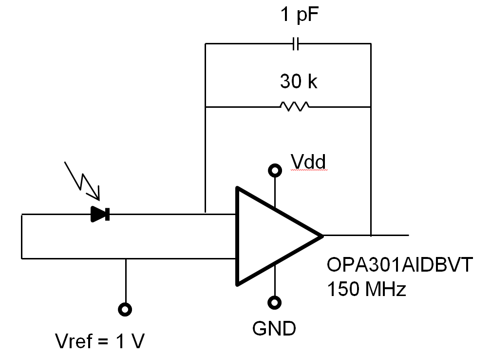
    My suggested circuit for the photo sensor would be: