This thread has been locked.

If you have a related question, please click the "Ask a related question" button in the top right corner. The newly created question will be automatically linked to this question.

LOG114 Tina-TI simulation and real behavior

Other Parts Discussed in Thread: LOG114, TINA-TI, TPS60400, TPS60240

I'm designing scheme with using of LOG114.

Task and scheme is rather typical: compression and amplification of photodiode signal.

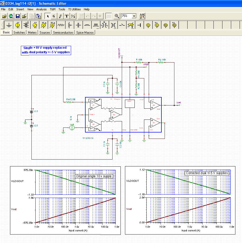
I'm starting with scheme from LOG114 datasheet (for dual-supply configuration), and calculated my parameters for input from 1nA to 1mA (6 decades), reference current 1uA (2.5MOhm resistor and 2.5V internal Vref) and 0 - 2.5V output. It gives me some reasonable R1, R2, Rg and R values:

R1 = 290k, R2 = 90k, R = 100k, Rg = 110k.

I'm entered scheme to Tina-TI and got very strange results: Vlogout is not where expected -- it starts from ~965mV, not from 1.25V, it crosses zero at ~400nA, not at uA, and scaled and shifted Vout is completely wrong too. Also, it could be seen, that Vlogout and Vout is not strictly logarithmic. When I add "Vref" to outout, I was shocked: Vref was not constant 2.5v, but was around 1,000145v for most of simulation space, and then "rockets" to 1.00017 (which gives non-logarithmic output on this interval).

When I replaced internal Vref with "ideal" voltage and current sources, simulations shows perfect results, as calculated, with perfect logarithmic transfer!

Is it defect in LOG114 model or my scheme completely wrong and real device will work as predicted by simulation?

  • Hi Lev,

    I am a little confused regarding your LOG114 circuit resistor designations. It appears you are using the TINA schematic designators for R1 and R2. Is R = R3 and Rg = R4? If you could provide your TINA file that would be helpful.

    Regards, Thomas

    PA - Linear Applications Engineering


  • My designations is taken from video about LOG114 (part 2). I've created scheme "from scratches," to better understand it working and stuff.

    File is attached:

    0334.log114-i2.TSC

  • Hi Lev,

    I believe I found the reason you are having difficulty with the LOG114 TINA Spice simulation that have resulted in the incorrect output range and other problems. You applied a single +10 V voltage source across the LOG114 V+ and V- connections. The dual supply configuration requires +/-5 V sources with the common between them connected to ground. You can see the output voltage results before and after this change in the TINA result shown below. Vout for your design is now 0 to 2.5 V.

    If you intended single supply operation than follow the connection information shown in Figure 2 of the data-sheet. Be sure to use the latest LOG114 TINA simulation model posted on the web. There was an early version that had some issues when simulating single-supply operation.

    Regards, Thomas

    PA - Linear Applications Engineering

  • Thank you! I'm planning dual-supply configuration with two charge-pumps, tps60240 and tps60400, as suggested in datasheet, so single 10V supply disconnected with ground  is only my negligence in simulator.

  • Lev,

    I am glad I could assist you. Good luck with your LOG114 application.

    Regards, Thomas

    PA - Linear Applications Engineering