This thread has been locked.

If you have a related question, please click the "Ask a related question" button in the top right corner. The newly created question will be automatically linked to this question.

Fast overdrive recovery time of OPA699

Other Parts Discussed in Thread: OPA699, OPA847, LMH6624, LMH6642, OPA656

Hello, I'm Luca.

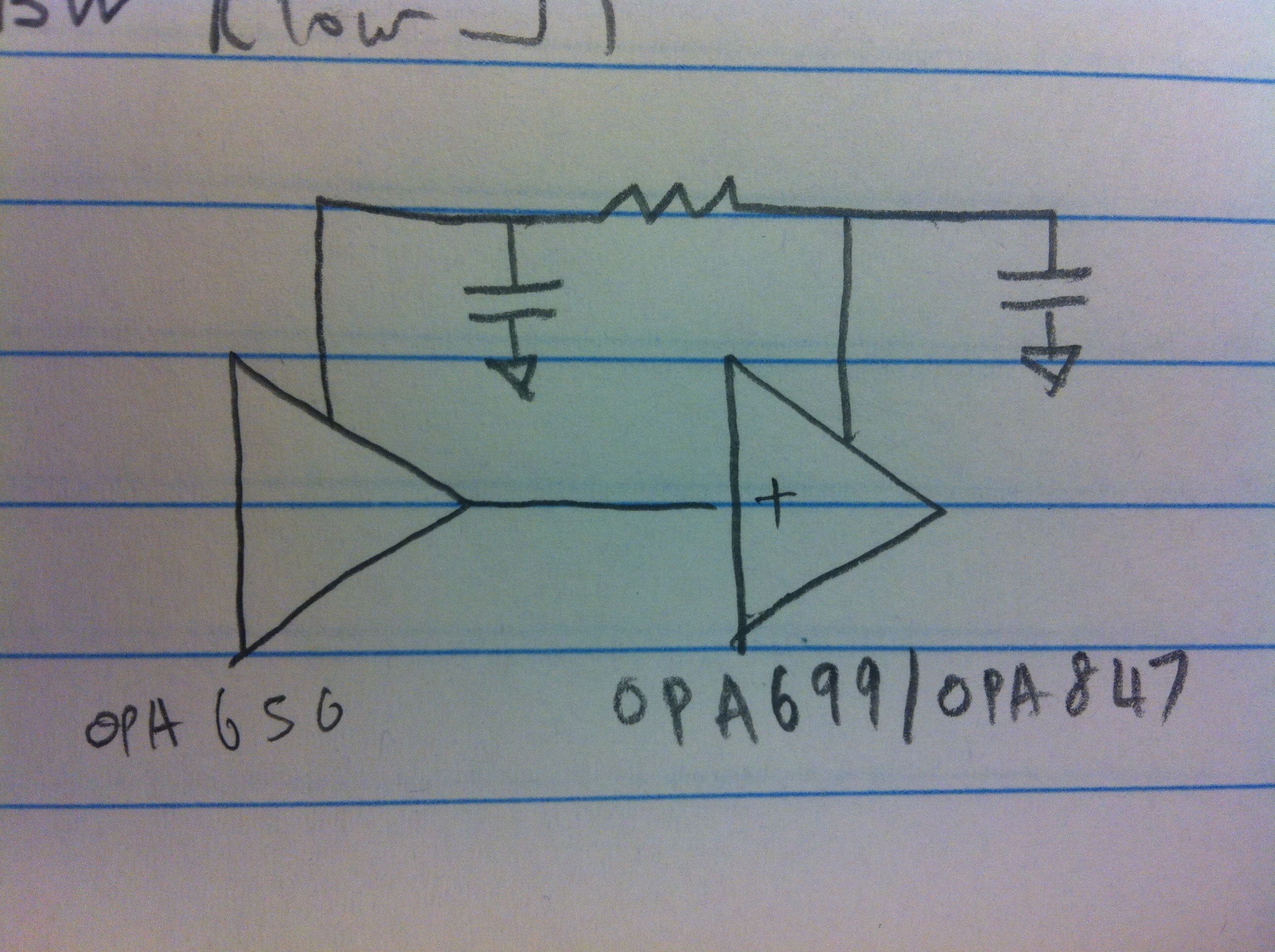
I'm designing a transimpedance with OPA699. Power supply is between 0V and +5V and the output limiters are +3V and +2V.

Everything work well untill the OPA699 saturate; in this case the recovery from saturation are very slow (hundred of nS) like other opamp.

My question is: is fast overdrive recovery time refer to the voltage exceed output limiters but that not saturate the OPA699?

Thanks a lot,

Luca

  • Hello Luca,

    Please see below for some information on the behavior of the OPA699 that you are seeing.

    When the OPA699 saturates and the op amp goes open loop, the + and - inputs are no longer at the same potential (no longer virtually shorted). For as long as the input has a large differential voltage (Vid), the output will remain saturated. The output only begins its recovery when this input differential voltage has been reduced such that the ideal output (Vout = Vid*Aol, where Aol = open loop gain) is within the op amp’s linear output range. For a regular op amp without a limiting function, the recovery time can be very long (ns to us), but for the OPA699 which has a limiting function at the output, this recovery time is limited to 1ns. This is the case when the OPA699 is configured in a regular non-inverting or inverting gain configuration. When the input signal changes and the input differential voltage reduces, the output quickly recovers from saturation and resumes linear operation.

    However, this is not the case in a transimpedance circuit. Even when the input current signal has been reduced into what would be the ideal linear region, the input differential voltage persists until the voltage on the capacitances at the inverting node has discharged sufficiently through Rf. Simulations will show this. See the attached “OPA699 TIA” Tina simulation.

    One way to take advantage of the limiting function of the OPA699 (if this is to go to an ADC, for example) is to cascade a TIA stage using a very low noise op amp such as the OPA847 followed by a regular gain stage implemented using the OPA699. The gain of the transimpedance stage should be limited to ensure that no input will cause its output to saturate. The OPA699 voltage gain stage can make up the rest of the gain without worry of saturating due to unwanted inputs. See the attached “OPA699 TIA composite” Tina simulation. The initial OPA847 stage provides a transimpedance gain of 7.1 kΩ and the subsequent OPA699 stage provides a gain of 6V/V. The total gain is 42.6 kΩ.

    For example, say the desired input signal is +/-20uA but there is the potential for the input to spuriously go as high as +/-100uA. With a TIA gain of 7.1kΩ the +/-20uA will be amplified to +/-140mV and the +/-100uA will be amplified to +/-710mV. This is within the linear output range of the OPA847. Since the original +/-20uA is the typical, desired signal, the gain of the OPA699 is set to 6V/V to amplify the signal further to ~1.7Vpp (for an ADC). The undesired +/-100uA signal (+/-710mV at OPA847 output) causes the OPA699 output to saturate, but the OPA699 quickly recovers back into linear operation.

    Another option is to use either back-to-back diodes on the input pair, or a single diode to keep the input within the Vlim range; however this would add capacitance on the input. This may work, but the above may prove to be the better solution.

    I hope this helps answer your question, please let me know if you have any further concerns.

    Regards,

    Ranji C. Bhola

    High-Speed Amplifiers

    3247.OPA699 TIA.TSC

    3782.OPA699 TIA composite.TSC

  • Thanks for your fast reply.

    My problem is the wide range of input signal (from 500uA to 0,5uA). The frequency of this digital signal is 1MHz.

    Your reply is clear: with normal transimpedance I can't reach my goal. I tried with the diode, but recovery time was always 300-600nS (too much for a 1MHz square wave). I have to find other solution. Do you know some op-amp or comparator that are useful for my application (1 MHz digital transimpedance with a wide imput range)?

    Thanks a lot,

    Luca

  • Hello Luca,

    Have you tried implementing the approach I detailed above in which you can try cascading the TIA stage using a very low noise amp such as the OPA847? Please see the above attached (OPA699 TIA Composite) TINA simulation for the data on performance.

    Let me know if that solution would fit your design and if you have any further concerns.

    Regards,

    Ranji C. Bhola

    High-Speed Amplifiers

  • Hello Ranji,

    I tried many solutions because my goal is to have the widest range of input current as possible (from 10nA to 500uA). I used in TIA stage LMH6642 (G=200k) with diode limitation and LMH6624 with two diode for voltage gain (G=1000). Noise and Jitter are my new problem, but the eye diagram (after a comparator) with a bitrate of 2Mb is very good.

    Do you think that my solution is a good choice? Or with OPA699 and OPA847 I'm able to reach better result?

    PS: I didn't use OPA847 because I hadn't still in laboratory. It will arrive next week.

    Regards,

    Luca

  • Hello Luca,

    The noise and jitter is definitely prevalent in your above mentioned solution, and it is stemming from the LMH6642, the jitter may be coming from the slew rate limitation in the LMH6624.

    I would recommend using an OPA656 instead of the LMH6642 as it has a high TIA gain, very low input bias current, and FET inputs to have very low noise; however there will not be rail-to-rail operation in that device. Then you may try an OPA699 or OPA847 to replace the LMH6642.

    The OPA699 would help the jitter if the cause is solely the slew rate limitation.

    The OPA847 would help the jitter if the cause is the Bandwidth limitation.


    As for the solution I mentioned to you in the previous post with the OPA699 and OPA847 the testing would be able to verify if this solution is a better option vs your solution above.

    For either case I would recommend powering the devices in the manner depicted in the attached image as this will help with PSRR & Oscillations. (Example below uses OPA656 and OPA699 or OPA847)

    Let me know if you have any further questions and how this turns out for you.

    Regards,

    Ranji C. Bhola

    High-Speed Amplifiers

  • Luca,

    For the above circuit, that resistor should be an inductor.

    Regards,

    Ranji C. Bhola

    High-Speed Amplifiers