This thread has been locked.

If you have a related question, please click the "Ask a related question" button in the top right corner. The newly created question will be automatically linked to this question.

Using OPA 2277 to drive N-channel MOS transistor (with negative feedback to stabilize the current)


Hello,

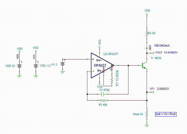
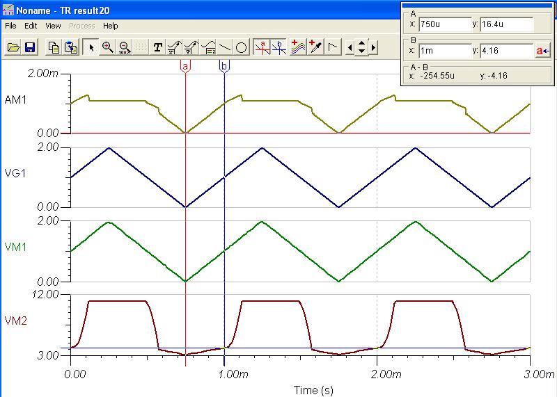
We are using OPA 2277 to drive a N-channel MOS transistor in linear mode. It is configured with negative feedback to stablize  the transistor current.  We provide the op-amp with dual power supplies (+12/-12).  The purpose of this circuit is to generate a stable current with the step voltage to the op-amp input.  How does the output common voltage affect the driving capability?  Are there any limitations?  The transistor threshold voltage is 2.0-4.5V.   The transistor can handle up to 90A at ambient temperature.

Thank you

Johnny

  • Hello Johnny,

    I believe your concerns about the output common-mode voltage come down to "Compliance" restrictions on the output of all current sources.  Basically you can't violate Ohms law and the current through the load must not produce a voltage that is larger than the maximum high-side voltage or "compliance voltage" of the current source.  Since you mention an NPN transistor I assume you're making a current sink so in this case the compliance voltage will be the minimum voltage on the collector of the transistor that doesn't force the NPN into a saturated operational state.  It will likely be the VCE voltage of the NMOS + any I*R drop through the sense resistor you have in your circuit. 

    For instance take a look at the circuit below.  It is a voltage controlled current source where the output current is set by Vin / Rset.  I believe your system may be similar.  In the first example the 10Ohm load causes the output common-voltage to be 10V.  The drop across the sense resistor is an additional 2V (10*199mA) so there is roughly 8V dropped across the transistor which keeps it operating in a linear range.  In the second example the load resistance has been increased to 1kOhms.  In this case it is not possible to continue to source 200mA because there is not enough voltage present in the system to support that current level through the 1k Load + the VCE drop of the transistor + the 10Ohm sense resistor.  The result is that the transistor is forced into a saturated region and no longer functions as desired. 

    Perhaps you could share a schematic of your circuit and we can take a better look in case I haven't guessed correctly at your circuit topology. 

    Normal:

    Complianced:

    Regards,
    Collin Wells
    Precision Linear

  • Hello Johnny,

    I made a mistake and built a circuit using an NPN instead of an NMOS.  However the same basic principle applies except that the circuit will now be limited by the Vds voltage of the NMOS instead of the VCEsat voltage of the NPN.  As you can see in the image below when the current through the load is around 80mA the NMOS gets cutoff because the Vd and Vs voltages encroach upon each other.  This occurs because the 80mA current through the 150 Ohm total resistance of Rload+Rset is equal to the supply voltage of 12V  ( 0.08A * 150Ohms = 12V) and the current simply can not go any higher in it's current configuration according to Ohm's law.  Since the input voltage to the OPA continues to increase the OPA tries to continue to close the control loop by increasing the gate voltage until the output reaches the OPA supply limits.  Please see the images below:

    Regards,

    Collin Wells
    Precision Linear


  • Collin,

    I found your post is very helpful.

    Thank you very much.


    Johnny

  • Hello,

    I'm glad it helped!

    Regards,
    Collin