This thread has been locked.

If you have a related question, please click the "Ask a related question" button in the top right corner. The newly created question will be automatically linked to this question.

THS4521 input when unpowered

Other Parts Discussed in Thread: THS4520, THS4521, TINA-TI

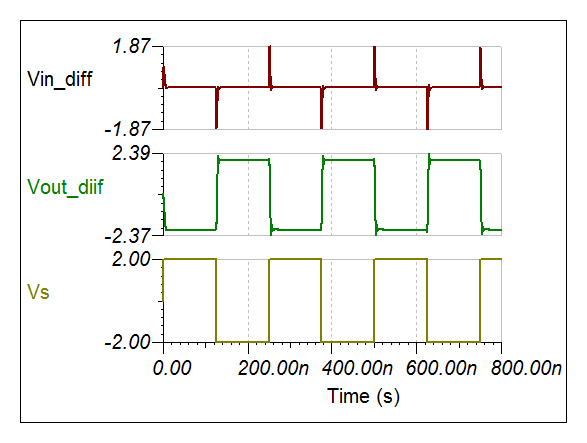
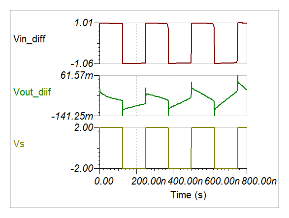
I'd like to use the THS4521 op-amp on a signal from another circuit with separate power. I'd like to be sure that no damage will be inflicted on the THS4521 when it is unpowered but receiving the input signal (+/-2V). The data sheet states a maximum current for the inputs of 10mA. Firstly, I am unsure if this is the only important factor to be aware of to prevent damage, and secondly I am unsure if this applies to the device while both powered and unpowered. I have read the post on the THS4520 (http://e2e.ti.com/support/amplifiers/high_speed_amplifiers/f/10/t/143225.aspx), which suggests that the input current limit is the important factor for that device and applies while powered and unpowered. Please could someone confirm the situation for the THS4521? Thanks.

  • Hello Arthur,

    I'm glad to see that you checked the forums for an answer first!

    The input current limitation applies to both powered and unpowered conditions. It is an estimated value based on process type, ESD type/size, IC layout, etc.

    It comes about when the internal ESD diodes turn on (about 0.7V to 1V differentially across the inputs) and they start to draw current away from the amplifier in order to protect the rest of the circuitry. As a rule of thumb, for the THS4521 these diodes shouldn't exceed 10mA of continuous current through them. Also note, that the maximum differential input voltage that these diodes can handle is 1V (as specified by VID in the Absolute Maximum Ratings table on the second page of the THS4521 datasheet), which would occur if the amp is running non-linear (applying a fast enough pulse to overdrive the amp for a brief period) or when the amplifier is not powered.

    In your case, if the input signal is a 4Vpp differential signal (1Vpp on each input terminal, assuming a gain of 1) you can violate this spec in two ways.

    If the amp is supplied with power and your input signal is a fast pulse (1ps rise/fall), then the amp will become non-linear for a brief period and violate the 1V differential input voltage.

    Additionally, if the amp is in a powered down state the output will not be able to track the input and it will cause a 2V differential voltage between the two input terminals.

    In both cases, the input protection diodes will be activated and then driven past the VID max limit, which can damage the device.

    I've also attached the TINA-TI simulation below.

    4555.THS4521_VID.TSC

    If you are running into the second case, then I would suggest using an attenuation network on the input stage to limit the amount of differential voltage seen by the amplifier.

    There is a good series of articles discussing this point written in the Analog Applications Journal:

    • Using fully differential op amps as attenuators
      • Part 1 - Differential bipolar input signal - slyt336
      • Part 2 - Single-ended bipolar input signal - slyt341
      • Part 3 - Single-ended unipolar input signal - slyt359

    Let me know if this helps.

    Regards,
    Luke LaPointe
    High Speed Amplifiers

  • Arthur,

    One additional thing to note. Once the input differential voltage exceeds the VID limit, the current will be redirected from the higher voltage potential input to the lower one. So the actual differential voltage seen by the input diff pair is clamped by the VID diodes, which the TINA model does not show. The input transistors should still be OK. But again, if you can avoid the situation all together, that would be best.

    Regards,
    Luke LaPointe
    High Speed Amplifiers