This thread has been locked.

If you have a related question, please click the "Ask a related question" button in the top right corner. The newly created question will be automatically linked to this question.

PGA309 problem with EEPROM

Other Parts Discussed in Thread: PGA309

Hello,

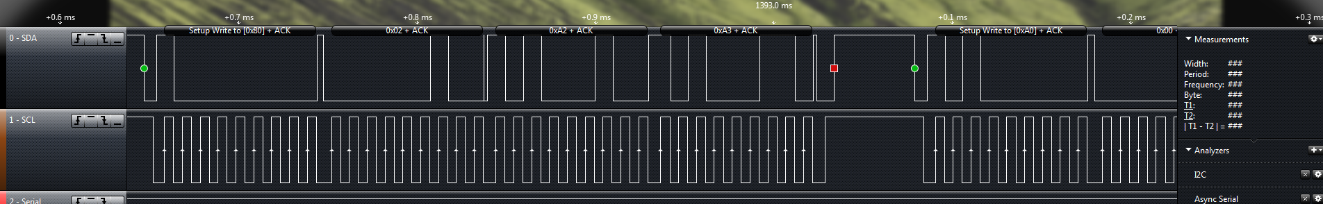
I got a problem with determine the EEPROM address. The PGA309 used default 0xA0 as I²C-Address. Now I tried to change 0xA0 to 0xA2 but it doesn' twork. I don't understand the communication to the internal registers with this device.

I tried the following:

First connect to PGA309 with Address 0x80

choose register 0x02 for addressing

now write 0xA2 into it.

Communication works well over I2C, I observed it with a logic analyser. The PGA309 responses but ignores all of my commands.

hope someone can help me.

  • Hello Andre,

    Sorry to hear that you are having an issue communicating to the PGA309. 

    So that I can better help you, please provide the following:

    1. The specific I2C transaction you are attempting to send (read or write command, what data, to which register of the PGA309 or EEPROM memory block)
    2. A scope capture or logic analyzer screenshot of the SCL and SDA lines

    Best regards,

    Ian Williams
    Linear Applications Engineer
    Precision Analog 

  • Hello Ian,

    Thanks for your command.

    I tried to write into register 0x02 of the PGA309 with device address 0x80. The Userguide said "Set EEPROM Address Pointer (02h)". I got an ACK from PGA309 after sending.


    Unfortunately I am not able to get a logic analyzer screenshot at the moment. The device is outside for testing so far.


    How would be the logical strategy?

    1)      Start with (0x80)

    2)      write(0x02) for selecting register

    3)      write new address of eeprom (0xA2) into register

    4)      stop

    I didn’t find any explanation how to set another eeprom address as 0xA0 via I2C. The PRG-Pin description seems different with respect to I2C programming.

    Might you give an example?

  • Hello Andre,

    In order to write to PGA309 register 0x02, you must follow the syntax below:

    1. Bus Idle: SDA and SCL lines idle high
    2. START condition: SDA transitions from high to low while SCL is high
    3. Write slave address: 0x80
    4. ACK by PGA309
    5. Register address: 0x02
    6. ACK by PGA309
    7. Register data byte 1: 0xXX
    8. ACK by PGA309
    9. Register data byte 2: 0xXX
    10. ACK by PGA309
    11. STOP condition: SDA transitions from low to high while SCL remains high

    Best regards,

    Ian Williams

  • Hello Ian,

    I got the device back today. I did already that what you said. Have a look at the screenshot below:

    The PGA gives an ACK but don't care about my sets. You can see it on the next start of transmission. It asks with 0xA0 again.

    What kind of value I have to set in the first and second register?

    Best regards,

    Andre Iwers

  • Hello Ian,

    Next problem is:

    I can read out the temperature and all other Registers [0:8] without any problems. But If I try to set e.g. register 0x01 to 0x0000 the PGA does not save the value. After setting these values and reading again the old value will be sent by the PGA309.


    Do I need to pull up any pin for programming via I2C?

    Best regards

    Andrw Iwers


  • Hello Andre,

    Your timing diagram seems correct, but there's a different issue. First, you do need pull-up resistors from SDA and SCL to VDD.

    Second, once the PGA309 completes its start-up sequence it will continuously read the EEPROM and overwrite its registers with the values stored in the EEPROM. In order for your writes to the PGA309 registers to take effect, you must first put the PGA309 in test mode. This is done by pulling pin 9, the TEST pin, up to VDD. Alternatively you can write directly to the EEPROM, in which case the PGA309 will update its registers with the new value you've written after you release it from test mode by driving TEST to 0V.

    To write directly to the EEPROM, follow the timing diagram given on p. 82 of the PGA309 User's Guide.

    Best regards,

    Ian Williams

  • Okay I found the error in the code and correct it. Now the PGA309 saves the date I did set before.

    Now I am a little confused about the description on site 77:

    There are six possible commands:
    • Set PGA309 Register Address Pointer (01h)
    • Set EEPROM Address Pointer (02h)
    • Write PGA309 Register (04h)
    • Write EEPROM (08h)
    • Read PGA309 Register (10h)
    • Read EEPROM (20h)
    See Figure 4-6 for timing details of these transactions.


    Can I access these registers via I2C? I thought I can but now I saw the internal overview on site 104. There are other registers with the same addresses depicted in Tabel 6-1.

  • Hello Ian,

    I already use 4k7 pullups and Writing to the EEPROM is not a problem. It works very fine.

    Question to the test pin:

    If I release it to GND the PGA309 will overwrite its internal registers by the values of the EEPROM. Okay I think I get it so far.

    If I write into the EEPROM some data (e.g. 0x0000 to address 0x01 and 0x02) it should be saved into the internal EEPROM of the PGA309 on address 0x01 and 0x02 right? (After next refreshing cycle of the PGA309)

    If I read the register after this refreshing cycle they are not equal to the external EEPROM values. They are constant anyway what I did before.

    Best regards

    Andre Iwers

  • I found a discussion about a emulation tool for the PGA309. Is it possible that I get a link for downloading it? So I can try something without bothering you that much.


  • Hello Andre,

    Regarding the table on p.77 - these are command bytes which are only used with the 1W interface (PRG pin). These commands do not apply when you are using an I2C interface.

    So if you write to the EEPROM, then read the values back, you are seeing the correct new values. However, if you read the PGA309 registers, they do not update with the new values in the EEPROM? I'll need to double-check the EEPROM-to-PGA309 register mapping to make sure this is being done properly.

    Can you link me the discussion for the PGA309 emulation tool? I'm not familiar with this tool.

    Best regards,

    Ian Williams

  • Hello Ian,

    The link to the discussion is the follwoing: click here

    I can send you a complete transmission protocol but you will need the software from saleae.com so that you can visualize it.

    The EEPROM values are definitively written and I can see them while the refreshing cycle is active. But if I read out the values of the PGA309 the old ones are still inside.

    Best regards,

    Andre Iwers

  • Hi Andre,

    This is the download link for the PGA309 calculator tool: http://www.ti.com/litv/zip/slvc073d

    I'll investigate this EEPROM-to-PGA issue. 

    Best regards,

    Ian Williams

  • Hello Ian,

    Thank you very much for the link. Could it be that the PGA309 only accept variables from the PRG pin?

    I actually did not try it, because I did not connect this pin to the µC.


    Best regards,

    Andre Iwers

  • Hello Ian,

    I don't know why but now the PGA saves the right values. I changed the hardware, completely.


    Now I have a question about programming this device correctly:

    • supply voltage: 3.3 V
    • my V_diff will be around 2.07 mV

    • and V_out max should be around 2.048 V (If possible without offset)

    At first I used the simulator for determining the correct values. My problem is the following:

    if I put V_in1 and V_in2 to the same potential like 1.05 Volts, I would say I should get an output voltage V_out  around 0 V. But I get V_sa on the output.

    Is ist possible to get 0 V to the output pin?

    Best regards,

    Andre Iwers

  • Hi Andre,

    The PGA309 output voltage range is from (GND + 0.1V) to (VS - 0.1V), so 0V output is not possible unless you apply a negative voltage to GND.

    With improper gain and offset settings, it is possible to force the output voltage to the rail even with 0V differential input. Typically when first starting to calibrate the device, we set the PGA309 for low gain and offset such that the output is near mid-supply (VS/2).

    Can you send a screenshot of your PGA309 block diagram with the various settings? 

    Best regards,

    Ian Williams