Because of the holidays, TI E2E™ design support forum responses will be delayed from Dec. 25 through Jan. 2. Thank you for your patience.

This thread has been locked.

If you have a related question, please click the "Ask a related question" button in the top right corner. The newly created question will be automatically linked to this question.

XTR111 - Current Limit Circuit Question

Other Parts Discussed in Thread: XTR111

I am working on a new product design using the XTR111 to implement a 4-20 mA current loop output.

The data sheet recommends two different external current limit circuits - Figures 37a and 37b.  The simpler circuit of 37a uses one extra PNP transistor (Q2), but has a potential downside of leakage current through Q2 causing an error in the desired output current value.  It appears that a high current will start to turn on Q2, which will decrease the gate/source voltage to Q1 and limit the current using Q1.

Question 1:  Is there an easy way to quantize the leakage current to determine the magnitude (percentage) of the error?  Is there an alternate but similar circuit that would have nearly zero leakage current until "tripped" by a high current?

The series circuit of 37b may be attractive because it eliminates the potential leakage current error.  However, now Q3 is in the direct current path with the MOSFET and provides the current limiting, which raises a concern about power dissipation.  My circuit design uses a heat sink on the MOSFET (Q1) to handle the steady-state loop power dissipation, which could approach 1 watt under worst case conditions (max loop current and high loop driving voltage).  When the loop current is low, Q2 should be OFF, and therefore Q3 should be saturated and have little voltage drop/power dissipation.  If, however, the MOSFET were forced into a fully saturated (low impedance) state for some reason, then it appears that the current limit circuit would kick in, and Q3 would have to dissipate all of the power.  I would like to use a SOT-23 packaged MMBT2907A for Q2 and Q3, as I don't have room for another large transistor with heat sink.

Question 2:  Is the current limit circuit only to protect against a short-duration turn-on transient, and therefore Q3 will have low average power dissipation, or should Q3 be sized for high current and require a heat sink as well?

  •  

    Hi James,

    Thanks for your interest in the XTR111. 

    Your understanding of the first current limit circuit is correct and current is limited by clamping the gate of the PMOS to the source which effectively clamps the PMOS drain-to-source current. 

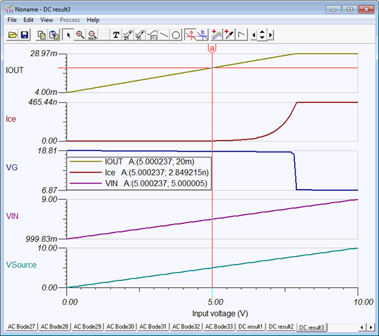
    The "leakage" current is really just the collector-emitter current (Ice) which starts to flow when the voltage drop across the 15 Ohm resistor begins to encroach upon the Vbe voltage of the Q2 transistor. 

    If you've designed the circuit correctly then the error due to the Ice current will be negligible until the output current begins encroaching upon the current-limit trip point which should be set well above the 20mA level.  I've included a simulation file and image showing this.  As you can see at the full-scale 20mA level, the Ice current is only 2.85nA at 25C.  The current will increase as temperature increases but you will have to make the design trade-off between the current-limit clamp level and the "leakage" current at 20mA.

    4118.XTR111_User_4-20_CL.TSC

    You are correct as well regarding the operation of the 2nd current limit circuit.  You are also correct that the series pass transistor will need to dissipate the full power in the current limit case.  If you do not have the ability to implement another large transistor with potential heat-sink then I would strongly consider the 1st circuit.

    Let us know if you additional questions.

  • Collin,

    Thank you.  That's exactly what I needed to know.  The first circuit is the best choice, especially given the extremely small leakage current in the normal (<=20mA) operating range.  In fact, if I am reading your simulation plot correctly, it appears that even at maximum Ice leakage current (at full current limit) the leakage error is <25ppm relative to full scale (20mA) Iout.

    Thank you for your prompt and very complete response!

  • Hi Collin,

    I am very new to XTR111 circuit. First of all i want to know why exactly do we need this external current limit circuit if you can explain please.

    thanking you

  • Hello Shri, Many people implement the external current limit as an additional safety measure in their system to prevent damage. There are some device protection reasons that are listed in the "External Current Limit" section of the product datasheet, starting on page 13. Please read through that and let us know if there are additional questions.

  • hello Collin,

    Thanks for your reply. Now i understood the working as i went through the datasheet and also the discussions over here. I just wanted to know whether this external current limit circuit can be implemented using anything else also or this MOSFET setup is the best option available ?

    Regards

  • Hi Shri,

    I don't understand what you mean by "implemented using anything else".  If you're using the XTR111 then one of the two circuits shown in the datasheet should work well for you.  If you're just looking for an external current limit circuit then choose the 2nd option shown in Figure 37 b "series current limit" which is a very simple but commonly used series current limit circuit.

  • Hi Collin,
    I'm working on a very cost-sensitive application using the XTR111, and I'm trying to save cost on the implementation of the MOSFET external current limit circuit. For this discussion I'll be referring to the circuits shown in figure 37 of the XTR111 datasheet.

    It seems to me that these circuits are there to protect for a transient situation that occurs when the Iout connection goes from being floating, to being connected to a very low impedance load. For the first few micro-seconds the MOSFET is still turned on and destructive current can flow. Please correct me if I'm wrong on that.

    The simplified circuit that I'm thinking to protect the MOSFET, would be like the one shown in figure 37(a), but removing Q2, replacing R6 for a short, and substantially increasing the value of resistor R7. In other words, the source of the MOSFET would connect directly to IS, the gate connects to VG, and the drain connects to a 10nF to ground, and a ~200 Ohm resistor in series with the output current.
    I understand that there will be a large voltage drop across the output resistor (200Ohm*20mA=4V), but if I'm powering with 24V and know that the voltage across my load will never exceed ~12V, then this drop should not be a problem.
    This output resistor also doesn't need to be high-power, just being able to take a surge that only lasts a few micro-seconds.
    What do you think about this solution?
  • Hi Juan,

    Your understanding of the requirement for the current limiting circuitry is correct. In the case when the load is open, the PMOS gate is driven to the maximum voltage. When the load is reconnected there is a short time before the gate capacitance is discharged that a very large current can flow which can damage the circuitry inside the XTR111.

    It's difficult for us to provide firm guidance that the protection scheme you're suggesting will work. With a +24V supply and a short circuit load, the 200Ohm resistor only limits the output current to 120mA which is well beyond the absolute maximum current through the IS pin of 50mA as stated in the absolute maximum ratings table. If you increase the output capacitance further to 100nF -470nF you may be able to slow down the output change sufficiently such that the control loop begins to regulate the output current before damaging currents can flow. That said, we would need you to test this out and provide us current probe waveforms of the output current while you connect/disconnect the load before we can make further judgment.