This thread has been locked.

If you have a related question, please click the "Ask a related question" button in the top right corner. The newly created question will be automatically linked to this question.

Ringing THS3202

Other Parts Discussed in Thread: THS3202

Hello everyone,

I'm having an usual problem with the THS3202.

If you look at my schematics here: 8004.schematics.pdf

You'll see that I'm cascading 2 THS3202, one with a total gain of 25 (2 times 5) and another with a gain of 5 (5x gain + follower).

If I connect GND to the left node of C22, remove C29 and measure the voltage (referenced to GND) at R23 I'll see a 460MHz ringing.

However, on the right side of the circuit (5x gain + follower), I find the usual behaviour of the THS3202

PCB layout is shown here:

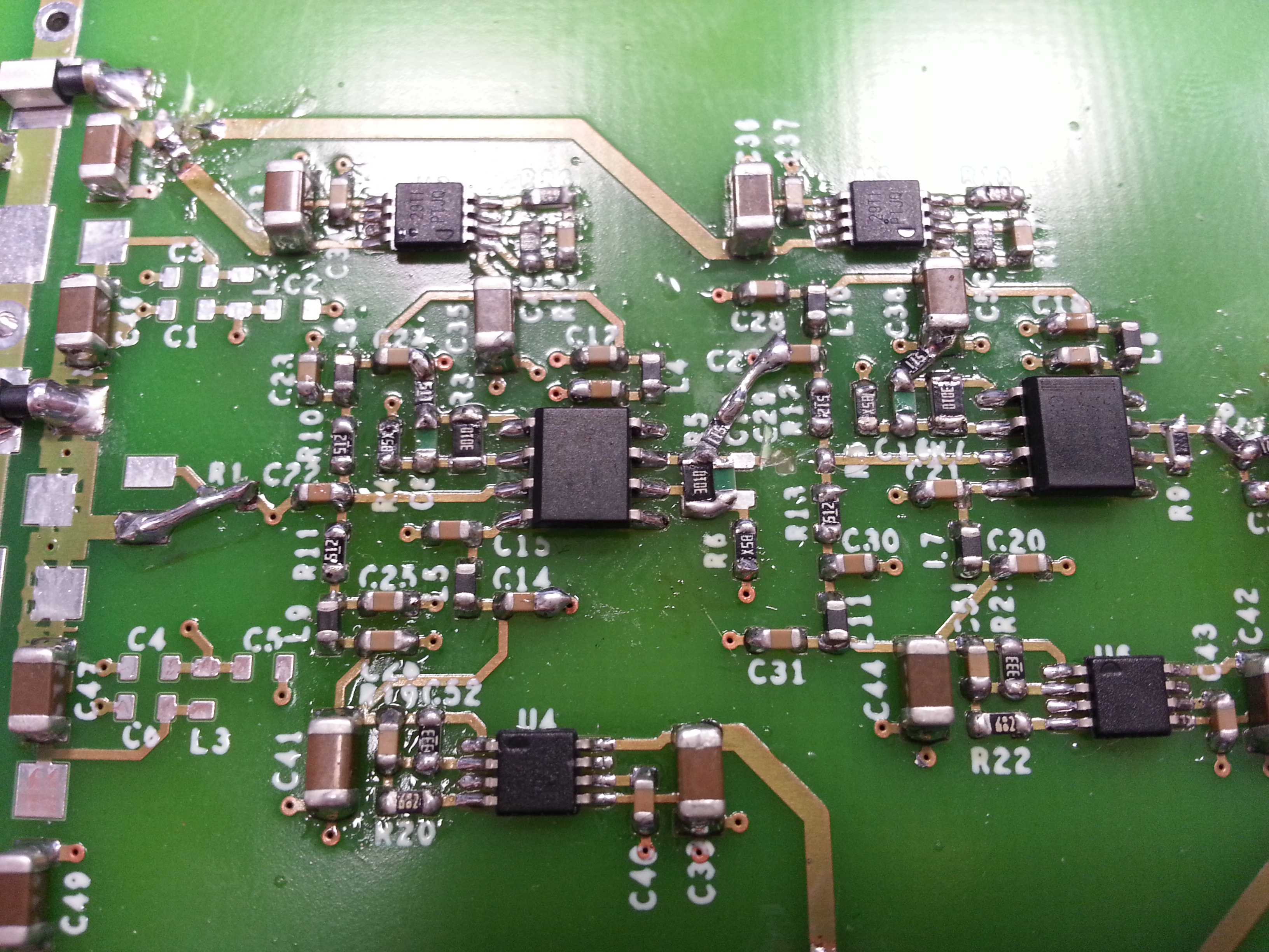
PCB is two layers, the other side is an uninterrupted ground plane, except for a void area around the text "R1".

Would anyone have an idea of what can cause this ringing?

Thanks a lot,

Mathieu

  • Matthieu,

    The most likely cause for the ringing you observe would be the light compensation of the THS3202 in a gain of +5V/V.  The datasheet, figure 10 & 11, shows ~2dB of peaking for 340ohm in the feedback resistance.  The capacitor across the feedback resistors, C8, C10 & C16 may help flatening the response, but in general it is not a recommended implementation for a current feedback amplifier as it may destabilize it.  The first THS3202 is likely to exhibit the problem more as there are 2 stages with the same peaking adding the overall peaking for that stage.

    I would recommend removing C8, C10 and C16 and increasing the feedback resistances to 420ohm.  Rg would then be 105ohm.

    Best regards,


    Xavier

  • Hello Xavier and thanks for your answer

    I removed C8 C10 C16, put 430ohms feedback resistors and a Rg of 110ohms but still got a ringing issue (ringing frequency is 430MHz now).

    Regards,

    Mathieu

  • Hello Xavier,

    It seems however that the ringing appears later than before.

    Would you suggest spreading out the gain between all the ths3202 (4 times 3.3)?

    I was also thinking of modifying the pcb in order to feed the output of the first opamp of the first ths3202 to the negative input of the second. Would that help?

    Regards,

    Mathieu

  • Mathieu,

    I have 2 comments on this:

    1) I notice the output of Amp A directly feeds into the + input of Amp B on both stages. In theory this is fine as the + input is high impedance. However, the input does have capacitances associated with it which can impact high frequency stability of the driver amp. It is recommended to place a 49.9-ohm resistor in series on each output to + input.

    2) It is possible that the Power supply filter circuit you have may be impacting this situation. PSRR at such high frequencies of any amplifier is not the greatest, and the power supply filtering can play a role. Sometimes experimenting with the Ferrite (some ferrites have very high Q, be sure a low Q ferrite is utilized) and/or the capacitors may have an impact.

    Cheers,

    Randy

  • Hi Mathieu,

    As you are changing the frequency of the ringing, you have most likely found the loop in which it is created.

    Changing the gain for each stage to be 4.35V/V should help.  The reduction in the PSRR at high frequency may be the cause for the ringing or some of it anyway.  This is describe in the following blog.

    http://e2e.ti.com/blogs_/b/analogwire/archive/2013/02/01/xavier-ramus.aspx

    Since you have separated the power supplies for the first THS3202 vs. the 2nd THS3202 and that the 2nd does not exhibit the problem, spreading the gain away from the first stage may help.

    To help isolate whether the PSRR/gain is the problem or whether the compensation of the amplifier is the problem, I would recommend to use 1kohm in the feedback for thsi test, to make sure that the ringing is not due to other parasitic issue such as a long trace on the non inverting input pin that may require isolation.

    If the problem still persist with 1kohm feedback with 5-5-5-1 gain, then spread the gain to 4.35-4.35-4.35-4.35, then reduce the feedback to 420ohm if the problem is still not present.

    feeding the negative input of teh 2nd amp would help only if the issue is related to board parastic, but would not help if the issue is due to the lack of PSRR of the amplifier at high frequency.

    Best regards,

    Xavier

  • Hello everyone and thanks for your answers,

    First, thank you Xavier for your blog article, and I think this is what might be happening in my case.

    Putting a 1k feedback resistor didn't solve the problem.

    Therefore I looked up the ferrites I used for these schematics (ones I had in stock): http://gb.mouser.com/Search/ProductDetail.aspx?qs=rvfpa0%252bU10NIg0zs9veElg== and it seems there are not ideal for high frequency applications.

    Which leads me to think that the noise introduced on the vcc rail might be too much.

  • Hello everyone,

    Things are getting quite weirder.

    I just implemented the following schematics on the existing PCB (without R28 and R30, and without powering U2): 7573.schematicsv2.pdf

    If I measure the voltage (coax cable with a 50ohms resistor at the end) at VIN2+ when powering the system, it will oscillate only after 6 or 7 seconds. If I measure the voltage after having powered the system it will be already oscillating.

    I also switched to RF ferrites (BLM18EG601SN1D)

    The oscillation (550MHz) doesn't really make sense to me as I only have a total gain of 3.38*3.38=11.42 at U1.

    Would anyone have an idea?

  • Hi Mathieu,

    I think you meant to say R23 and R30 are not popuplated.  R28 is the feedback resistor of an amplifier, so it has to be in place for you to have a gain.  Note that if R30 is not present the gain will only be 3.38V/V on each amplifier.

    I would start with overcompensating the amplifiers by setting Rf to 1k and using a 100ohm load.  If the issue is still present, I would remove L9 and L9 and replace them with short.  You will see the switching frequency from the power supply.

    When you probe, are you using an sicolloscope to see the oscillation?  Is the probe capacitive, say 10pF?  If yes, the issue could be the loading.  You should isolate the probe capacitance by inserting a 100ohm series resistor between the point you want to measure and the probe.

    Best regards,

    Xavier


  • Hi Xavier,

    Indeed you are right about R23 & R30. 3.38 is wanted & correct.

    I am using a Tektronix 3GHZ 10Gs/s oscilloscope, with a 50ohms in series at the end of the coax (at the PCB side)

    Changing rf to 1k didn't solve the problem.

    I'm currently making the version 2 of the board.

    Regards,

    Mathieu

  • Hello everyone,

    It turns out that we can't power the THS3202 using +7/-7V when using the SOIC package.

    I'm quite disappointed of seeing no warning in the datasheet. Using a homemade heatsink, the temperature difference between the die and the top of the SOIC package is too big, and therefore the THS3202 oscillates.

    All my "adventures" are mentionned here: http://www.limpkin.fr/index.php?post/2013/03/01/Amplifying-nanosecond-pulses-for-quantum-physics-experiments

  • Hi Mathieu,

    good work. I like it :-)

    As you said, it's a temperature issue. However it's not related directly to the SOIC package that can work at the rates you've mentioned as long as you don't exceed the maximum. If you check some datasheet figures you´ll see how temperature degrades offset, output current source and also the power supply rejection ratio - a potential cause of the described oscillation.

    regards,
    gaston