This thread has been locked.

If you have a related question, please click the "Ask a related question" button in the top right corner. The newly created question will be automatically linked to this question.

Current Sensing using INA118

Other Parts Discussed in Thread: INA118, OPA177, TINA-TI, INA333

Hi,

I am trying to measure the current on high side using a shunt resistance. During certain stages, the voltage across the shunt resistance could go as low as 60uV. So, I chose the INA118.  The gain I have set is 10.

The problem that I am having now is that when Vin+ = Vin-, the output voltage that I am seeing is 40mV.  Hence, I am unable to view any input signal when Vin+ -Vin- < 4mV. I am going to try and do the offset trimming suggested in the datasheet. I already tried connecting a DC power supply at the REF pin and found no change. Am I doing something terribly wrong?

Thanks in advance.

  • Hello Genie,

    I suspect you're saturating the output stage of the device. The output swing of the device depends on the supply voltages, gain, reference, and input common-mode voltage. Please take a look at the graphs on page 4 of the data sheet entitled "Input Common-Mode Range vs. Output Voltage."

  • Hi,

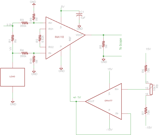
    I chose 5V as the INA118 supply for an input common mode of 3.3V and I think the input is in the operating range. I am including my schematic in here.  What I am trying to do is a High side current sense of an IC.  Rx is chosen such that when the IC is active, the voltage doesn't drop much below the datasheet specs (Vx > Vmin = I_spec *Rx). The Voltage range for measuring standby currents are as low as 60uV. Hence I chose INA118 as I mentioned before. I connected the OPA177 as shown below but I am unable to trim the 35mV. It isnt lowering at all. Could you tell me if I am doing anything wrong?

  • Hello genie,

    By '...unable to trim the 35mV' and 'it isn't lowering at all' I believe you're trying to get the output of the INA118 to exactly 0V.

    If so, that is to be expected. The output stage of the device cannot reach 0V when the supplies are 5V and GND.  Please refer to the Output section of the specification table and the aforementioned graphs.

    Instead of trying to force the output to 0V, a small reference voltage applied to the REF pin becomes your '0V'.

    Please take a look at the attached TINA-TI simulation.

    Finally, please note that the input offset voltage of the device for G=10 is +/-100uV or +/-225uV (depends on grade).  Perhaps you'd be interested in a lower initial input offset device like the INA333.

    genie.TSC