Because of the holidays, TI E2E™ design support forum responses will be delayed from Dec. 25 through Jan. 2. Thank you for your patience.

This thread has been locked.

If you have a related question, please click the "Ask a related question" button in the top right corner. The newly created question will be automatically linked to this question.

There is someting wrong with application note sbfa005 about UAF42

Other Parts Discussed in Thread: UAF42, OPA627, TINA-TI, DAC7811, DAC7800, OPA131

A few days before, I wanted to design a programmable filter with UAF42. Luckily,(or unluckily) I found an application note which name is 'Digitally Programmable, Time-Continuous Active Filter ' on website http://www.ti.com/product/uaf42. After I finished the circuit referring to the application note, however, the output wave isn't correct.

So, I analyzed the application note carefully. I found there's a mistake in it.

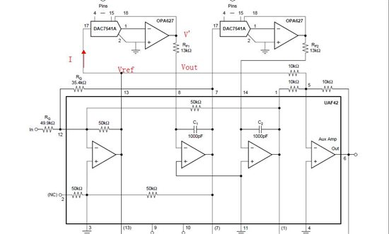
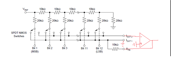
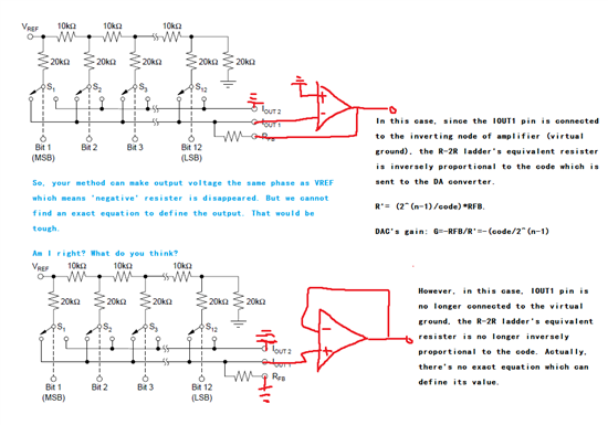
We can change UAF42's cutoff frequency by changing the resister between pin 13, 8 and pin 14, 7. Furthermore, if we want to create a 'programmable' filter, we can use a DA converter to change the equivalent resister between pin13, 8 and pin14, 7, just like the figure below.

The application note is theoretically right, but actually, it doesn't work.

Here are my equations:

I=(V'-Vout)/Rf1;

V'=-code/4096*Vref;

Requ=(Vref-Vout)/I;

Vout≈0;

Hence,

Requ=Vref/I

=Vref/(V'/Rf1)

=Vref/V'*Rf1

=-4096/code*Rf1

So, the equivalent resister Requ between pin 13, 8 is a 'negative' resister. It's amazing! Of course the circuit won't achieve our desired function.


After I added a voltage inverter between OPA627's output pin and Rf1; the circuit finally worked very well.


My analyses are listed above. What do you think?

If the application note is really wrong, I hope TI's employee can correct the application note to prevent others make the same mistake.

  • Hello Zhe,

    Please understand that the UAF42 programmable active filter application was developed almost 20 years ago and the fellow that did the work has retired. Therefore, we are having to reinvent the wheel (per se) to understand how it works. The circuit has been published in several different journals and I presume applied without any problems being reported that we are aware of; that is until now. 

    I carefully went over your derivation of Req and came to the same conclusion; the equivalent resistance does equate to a negative resistance. That happens because of the inversion introduced by the OPA627 inverting amplifier and that does seem like that would be a problem for the circuit; however, do note that there are two of these Req resistances in the complete filter topology. When discussing this application circuit with one of my colleagues he suggested that it may be because of the two negative Req resistances that the circuit behaves as expected. The two inversions within the feedback paths may result in the correct phases being maintained and results in the expected filter response.

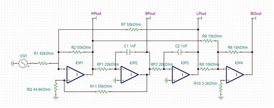
    To test that idea, we took a basic UAF42 filter circuit and ran a gain vs. frequency plot using our TINA-TI Spice simulator. Then, an ideal inverting-operational amplifier stage was added in series with each of the RF1 and RF2 feedback resistors. Another gain vs. frequency simulation was made. The simulated responses were identical for both circuits.

    Did you test you filter with a DAC/ inverting amplifier in both RF circuit spaces, or in just one? If you applied it in just one, then we expect you would have to invert the amplifier output to maintain the correct phase relationships.

    Regards, Thomas

    PA - Linear Applications Engineering

  • Hello Thomas,

    Thanks for your reply

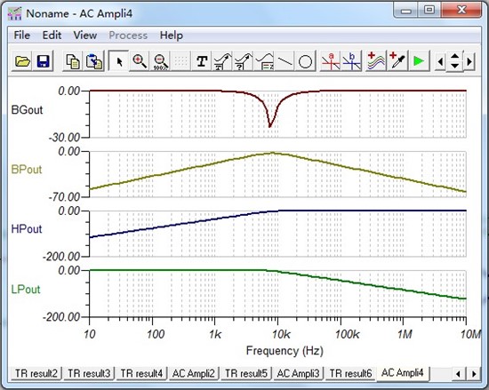
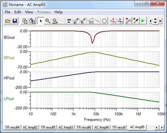
    I simulated with the circuit with ideal inverting-operational amplifier and RF1 and RF2 as you did. The AC Transfer Characteristic simulation's responses were the same as circuit only with RF1 and RF2 .

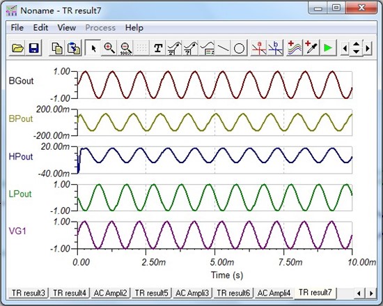
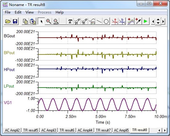
    BUT, have you ever tried the transient simulation? The wave is completely wrong.

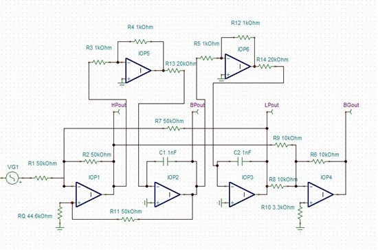
    circuit1:

    AC Transfer1:

    transient1:

    circuit2:

    AC transfer2:

    Transient2:

  • I used two DAC7811s.

    In actual circuit(not simulation), when I use only Rf1,Rf2 resisters or just connect DAC7811's 18pin which is connected to the feedback resister inside DAC7811 to Rf1 omitting OPA627, the circuit worked very well. But when I connect OPA627('negative' resister occurred), the wave is wrong.

    I don't know why the AC transfer characteristic simulations are the same, while transient simulations are not. This phenomenon has happened in several different circuits I simulated. I think it's relevant to the TINA's simulation algorithm.

  • Hello Zhe,

    This is proving to be a tough one. I simulated the UAF42 application using the added ideal operational amplifiers and found the transient behavior to be the same as what you found. I then substituted real, non-ideal operational-amplifier models for the op-amps and also tried changing some of the transient analysis parameters. Nothing changed the outcome. The transient analysis is a more stringent test than the ac analysis and when it produces a null output then that is a pretty good indicator that things aren't right.

    I would like you try something with your built-up circuit. Return the circuit to the original configuration shown in the applications bulletin. Except now reverse the pin 1 and pin 2 connections of each DAC7541A so that each pin 1 is grounded and each pin 2 drives the respective OPA627 inverting input. The reason I am suggesting this is pin 2 current is the inverse of the pin1 current. I think this may provide the needed inversion that you accomplished with the inverting amplifier stage you added after the OPA627.

    Let me know what you find.

    Regards, Thomas

    PA - Linear Applications Engineering


  • Er......I think you have made an abvious mistake.

    Pin 1 cannot be grouded,since the feedback resister inside DAC is connected to pin 1. Here is the figure:

  • Hi Zhe,

    Yes, an oversight on my part. It looks like a precision 10 k feedback resistor would have to be added to the OPA627 I-V converter.

    Regards, Thomas

    PA - Linear Applications Engineering


  • Hi Zhe,

    I think I have an easier way to accomplish what we are after. The OPA627 needs to be configured as a non-inverting I-V converter; instead of an inverting I-V converter. Here is the revised connection for each of the two synthetic resistor sections:

    1. Leave DAC7541A Iout 2 (pin 2) connected to ground as the original UAF42 application schematic.
    2. Ground DAC7541A RFB (pin 18).
    3. Connect the OPA627 as a unity-gain buffer.
    4. Apply the DAC7541A Iout1 (pin 1) to the OPA627 non-inverting input.
    5. The OPA627 output drives the RF as it did in the original circuit.

    What do you think?

    Regards, Thomas

    PA - Linear Applications Engineering

  • Hello Zhe,

    It is good to hear from you again. Well, all I can say is this has been a learning experience for both of us!

    Yes, I do see my proposal fixes the inversion problem but creates the DAC code issue you mention. Thus, it appears that the only practical ways to resolve the inversion problem are; 1) use the I2 output current and add an external resistor to the OPA627 I-V converter as I proposed at one point, or 2) use the I1 current and leave the op-amp out of the circuit altogether - a technique you had suggested, tried and found to work.

    I actually found evidence of the second being applied in another product's data-sheet. Figure 9, on page 13 of the DAC7800 data-sheet, shows a digitally programmable (fc, Q and gain) active filter using the UAF42 where the fc and gain adjust do not include the I-V operational amplifiers. The filter's information on page 10 mentions that the ladder resistance cannot be less than 10 k and that limits the top-end frequency to 16 kHz.


    Regards, Thomas

    PA - Linear Applications Engineering 


  • Thomas Kuehl said:

    To test that idea, we took a basic UAF42 filter circuit and ran a gain vs. frequency plot using our TINA-TI Spice simulator.

    Thomas or anyone,

    Can you please share your TINA-TI simulation file for the UAF42?  I need to do similar gain vs. frequency analysis for our design using the UAF42, and I'm new to both the UAF42 and using TINA-TI Spice, so any assistance with a starting file would be appreciated.

    Regards,

    Robert

  • Hi Robert,

    During the time of the original DAC controlled UAF42 notch filter thread I found that the TINA simulation model was not giving the correct notch filter responses. I do think it was okay for other filter responses, but not for the notch. Rather than chancing erroneous simulation results I built a discrete UAF42 model using ideal operational amplifiers. That worked well, but ideal operational amplifier models give ideal results and something real can be missed.

    I searched and identified an operational amplifier that is reasonably close in dc and ac performance to those used in the UAF42. I reconfigured my ideal UAF42 model to use four, discrete, OPA131 operational amplifier models. They should provide a more realistic responses than the ideal operational amplifiers.

    You will find the discrete UAF42 model in the attached TINA file. You can change the resistor values and connections to whatever is required for your specific response.

    Regards, Thomas

    PA - Linear Applications Engineering


    UAF42_60Hz_notch_03.TSC
  • Thanks Thomas.  I appreciate that you took the time to start me off on the right foot, and the more realistic response.  The calculations we'll use the simulated response in would be sensitive to any deviation from actual. 

    BR,

    Robert

  • Thomas,

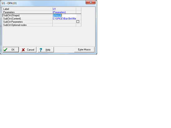
    My circuit based on the example you provided wasn't working.  So I looked closer at the op-amps.  I noticed they're labeled OPA131, but are referencing a file called C:\SPICE\Burr Brn\New\OPA121\OPA121E.MOD in SubCkt-(Content).  At first I didn't have that file locally.  But I found it on the web, and put it in that exact same directory, since it wouldn't take a directory location change in SubCkt-(Content)).  But yet the circuit still doesn't work, as if the op-amps aren't working.  Should that be all that's needed, i.e. point to OPA121E.MOD?  I've attached a picture of the op-amp properties.  Please advise.

     Robert


  • Hi Robert,

    I think I had pulled the OPA131 model from the product web page and that is how the association with the OPA121 model came about. It looks like you overcame that issue.

    The problem with your circuit was the power supplies were not transferred over form my original circuit. I added them back into your circuit and it runs. This is an easy mistake to make and I've done it more than once.

    I found an OPA131E model in my library which is an enhanced version of the OPA131 model. I am not sure about the details, but it was an update to the earlier one. I plugged them into your circuit.

    If you get stuck, let me know and I'll help.

    Regards, Thomas

    PA - Linear Applications Engineering


    UAF42_notch_02.TSC
  • Thanks again,

    Robert

  • Hi Thomas,

    Attached is our latest filter design.  It's a bandpass filter, intended to pass only 60 Hz.  However, even though the TINA response looks fine, during actual runs, it's not stable.   It doesn't blow up, but the ampltiude is modulated significantly, i.e. up and down, up and down, around a median value.  Can you provide any insight into why, or suggestions on how to fix this?

    Regards,

    Robert

    2161.20130819 bpf.TSC

  • Hi Robert,

    So it appears you are attempting to synthesize a 4-th order, 60 band-pass. Based on the current component values an ac simulation shows a gain of about 1.21 V/V at 60 Hz. It looks like the filter is taking about 500 ms for the amplitude to stabilize. If you do a transient analysis with a time anything less than that the amplitude will not be stable and will be in the process of increasing toward the final stable value.

    Please provide me the gain, type of response (Butterworth, Bessel, Chebyshev, etc), bandwidth, Q, etc. How are you determining the component values?

    Regards, Thomas

    PA - Linear Applications Engineering

  • Thomas,

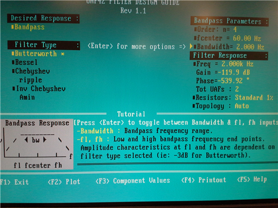
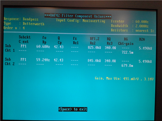
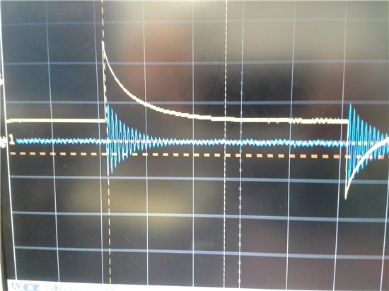
    We are using the FILTER42.exe program associated with this part.  I've attached 3 pictures that hopefully answer your questions:

        1) the initial design screen

        2) the resulting components

        3) a scope trace, showing the approximate 500 ms step you predicted

    Addition information from today is that the instability (if that is what it is) may be environment dependent, i.e. it was worse last week then today.  The circuit itself is on a breadboard, during the debugging phase.  So there is question about susceptibility to environment noise.

    Thanks,

    Robert

  • seemed to have lost the pictures, so trying again....

  • Hi Robert,


    I am glad to see you found the original FilterPro software that has the UAF42 filter synthesis capability.

    The bandwidth of the band-pass filter is very narrow, 2 Hz. We can see from the software screenshot that the Q of each stage is 42.2 which is very high. Ringing in an analog filter follows the Q; the higher it is the more sustained the ringing will be when an impulse applied to the filter input. I expect that lowering the Q would help reduce the ringing. Filters are often designed primarily for their frequency response, and their phase and time responses may suffer as a result.

    When we look at the number of loops in the filter it doesn't surprise me that it takes upwards to a half second for the amplitude to stabilize. Especially when considering the ringing in the circuit. I simulated the filter using ideal operational amplifiers and the amplitude stabilization time was about the same as using the OPA131 amplifiers. A high Q circuit can be sensitive to an environmental condition such as temperature. That may be what you are observing when you mention susceptibility to environment.

    Regards, Thomas

    PA - Linear Applications Engineering

  • Thomas,

    We only need to have sufficient attentuation by the 2nd harmonic, i.e. 100 or 120 Hz.  I widened the pass band to 6 Hz, and dropped the Q's to 14.15, which per your advice, might help.  According to TINA, the attentuation at 120 Hz decreased from -65 dB to -52 dB.  That might stll be ok.  Otherwise, I can play with tradeoffs, like 4 Hz passband, etc.  Or as a last resort, add another 2 or 4 poles, to keep the lower Q, while achieving sufficient stop band attenuation.

    Thanks,

    Robert

  • Hi Robert,

    You are completely on track with your thoughts about lowering the Q. If you can accomplish the required 2nd harmonic attenuation by widening the bandwidth and decreasing the Q, the circuit will have faster impulse response and less ringing (providing you stay with the same filter response, i.e. Butterworth). Increasing the filter order may not be desirable from a component standpoint, but it will allow you to achieve higher 2nd harmonic attenuation with a lower Q filter.

    This morning I tried taking the original circuit requirements and synthesized a two-stage Sallen-Key 60 Hz band-pass filter. I used a linear-phase filter response with the hope of improving the impulse response. This filter required two operational amplifiers and 14 passive components. It was set up in TINA and compared to your original UAF42 design. Interestingly, but as expected, the amplitude stabilization time and impulse response behavior - ringing - were very similar for these two completely different topologies. You can see the results in the attached file. It solidifies the idea that another, different filter approach is necessary to achieve the goals.

    Regards, Thomas

    PA - Linear Applications Engineering

    60Hz_sk_LinPh_01.TSC
  • Thomas,

    That is interesting, how the two distinct topologies turned out so similar.  In that case, I'm happy to report that I took our original topology, via TINA, and doubled the bandpass, from 2 to 4 Hz.  The Q was halved, the resistor changes were minor, attentuation at 120 Hz still adequate and it appears there is little-to-no ringing now.  And as a result, little-to-no amplitude modulation seen with the 2 Hz bandwidth design.  If that holds up over more testing, I'll consider it a wrap on this portion of our effort, but will post back if something else comes up.  Next step will be to get it off the proto board and onto a PCB.

    Thanks for the help and information.  

    BR,

    Robert

  • Hi Robert,

    The reduced Q looks to be a good solution and its nice that you don't have to increase the filter order to achieve the 2nd harmonic requirement.

    Do let me know how everything works out once you get the PCB version playing.

    Best Regards, Thomas

    PA - Linear Applications Engineering