


Hi, TI Engineers
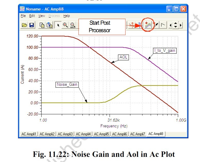
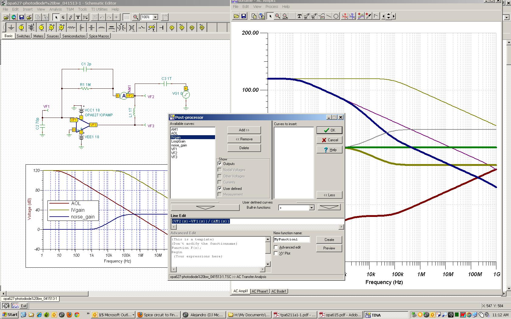
In "analysis and measurement of intrinsic noise in op amp circuits,Part XI:Photodiode Amplifier Noise" wrote by Art Kay and Bryan Zhao, page11, it gives a circuit to generate the noise gain , Aol and current to voltage gain.
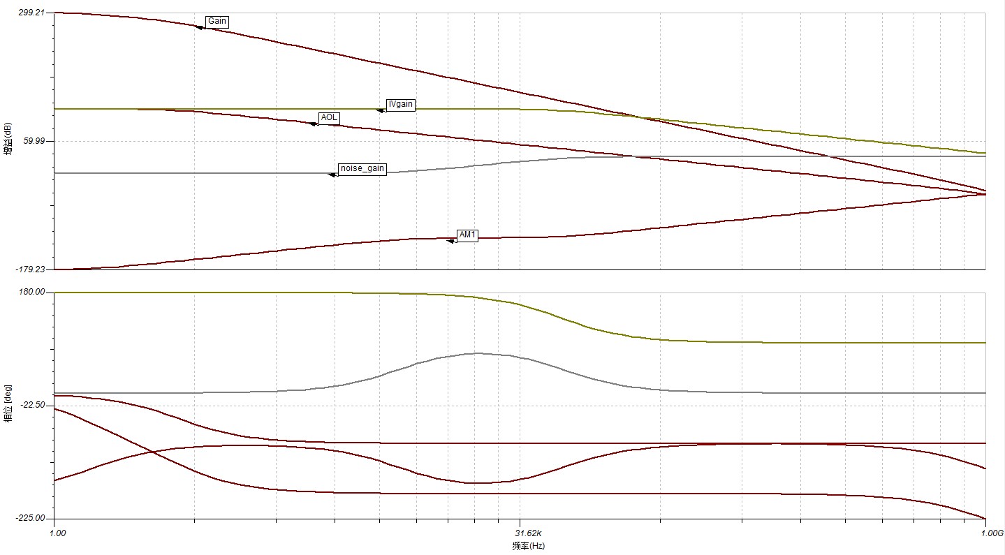
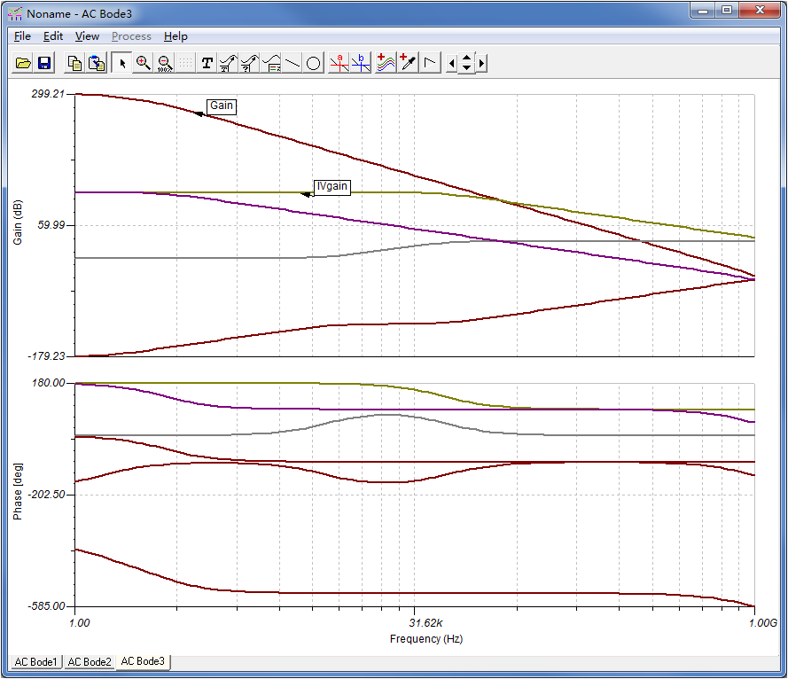
I used TINA to bulid the same circuit, but I didn't got the same plot(FIG.11.22)
Attachment is the TINA file. I think I may set some wrong parameter of the opa627.2260.FIG 11.20.TSC
 vs
vs 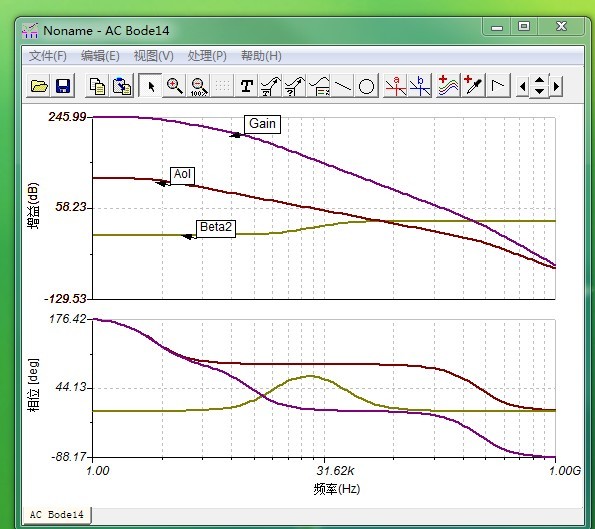
Regards!
Eva


