This thread has been locked.

If you have a related question, please click the "Ask a related question" button in the top right corner. The newly created question will be automatically linked to this question.

XTR111 Current Limit Trouble

Other Parts Discussed in Thread: XTR111

Hello,

 can you please help on below questions (bottom of mail)  from my industrial end customer FESTO.

Thanks a lot in advance !

 Regards

Günter Fettig


 Reference: Datasheet XTR111, Figure 3a

Using the XTR111 as current output (4-20mA) for a new circuit, I am struggling to design the external current limit perfectly. Only the circuit 3a (gate controlled current limit) is possible in this application because there is no possibility to implement a heat sink for a second large transistor as it would be necessary for the serial current limit 3b.


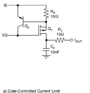
Thanks to a discussion on the Ti Website Link, I think that I understand the principle of this current limit correctly. With currents well above 20mA, the voltage drop at R6 should reach the Base-Emitter (turn)-on voltage of Q2. This will clamp the gate of Q1 to its source, and so limiting the possible current flow through Q1 (to the load).

 I want to use a BC807-40 PNP transistor for Q2. The circuit should be working correctly from -25°C up to (at least) +100°C. With higher temperatures, Q2 will turn-on much earlier and so limiting Iout to lower values. With the datasheet-information (figure 38 and chapter “EXTERNAL MOSFET” ) I made some simulations of the current limit and found out, that R6=18R would be a good choice.

 Parameters:

Temperature -25°C ... +125°C (50°C steps)

VSP = ~IS = 30V

VG = VSP-16V = 14V

Internal resistance of VG-Drive = 3k

Q1 = BSS84 (for simulation only, design will be with a BSS192, no simulation model for this)

 Simulation:


Results:

I_RLoad is limited to max. 40mA (-25°C) and min. 24mA (+125°C)


I_VSP (the current that should be limited to 50mA to protect the XTR111) is restricted to max. 44mA (-25°C) and min. 28mA (+125°C)


 Using and testing exactly this circuit in the lab, I can see that the I_RLoad current of 20mA is starting to decrease with higher temperatures starting from +60°C. The reason (with a very high certainty) is the external current limit: If I remove Q2, everything works fine up to +120°C, with a nearly stable current at the output. I already tested to use R6=15R with no real difference in the behaviour.

 Additional information: At  high temperatures (+110°C), Vin is stable and R_Set is stable, R6 is stable.

 Question 1: Is there anything fundamentally wrong with my simulation model, or with my understanding of the circuit?

Question 2: What resistor would be recommended by the experts using a BC807-40? Is the BC807-40 a completely wrong choice?

Question 3: What else could be the reason for this behaviour?


  • Hello Gunter,

    Question 1: Is there anything fundamentally wrong with my simulation model, or with my understanding of the circuit?

    Your understanding of the circuit is correct.  As the current flow increases through the 18R resistor, it creates an increasing voltage drop.  Once the voltage drop is high enough ( > Vbe ) to allow the transistor to conduct current from emitter to collector, the gate-to-source voltaeg of the PMOS device will be limited, limiting the possible current flow from source to drain.

     Question 2: What resistor would be recommended by the experts using a BC807-40? Is the BC807-40 a completely wrong choice?

    I don’t believe the BC807-40 is a completely wrong choice for this design, but since it’s not working we may want to try a different model.  We frequently recommend very basic transistors for this application such as the MMBT2907 and the BC807 has similar characteristics.  I downloaded the datasheet for the BC807-40 from several different manufacturers and they seem to correlate fairly well.  On average, with a collector current around 30mA, the devices seem to have around -1.9 -  -2.2mV/C of temperature coefficient on the Vbe(on) voltage which is pretty standard for BJTs and all diodes.  Therefore over a 125C temperature range (-25C – 100C) the expected change in Vbe will be from -240mV to -275mV.  Therefore to determine the change in clamping current, we can divide this voltage change by the sense resistance, and come up with between -13.5mA to -15.3mA as the temperature increases.  Your SPICE results seem in line with these calculations. 

     The calculations above were to determine where the effective clamping current would occur.  As noted in the post you referenced, there is a current that flows through the current limiting transistor well before the device turns on enough to turn off the PMOS.  This is likely the error current you’re seeing at 60C.  I would recommend trying a different BJT and see if the device behaves a little better.  Perhaps a BJT with lower gain (hfe) would show less error before it turns on fully.

     Question 3: What else could be the reason for this behaviour?

    You are correct that the reason is the current limiting circuit, there shouldn’t be anything else going on if the issue is resolved when the current limiter is removed.  Designing this circuit to properly limit at low temperatures while not causing error at higher temperatures is challenging as you’ve experience.  The XTR111 will operate within the datasheet specifications over the full operating range of the device. 

     I hope this answered the questions.