This thread has been locked.

If you have a related question, please click the "Ask a related question" button in the top right corner. The newly created question will be automatically linked to this question.

How to stabilize OPA551/OPA551 with capacitive load?

Other Parts Discussed in Thread: OPA552, OPA551

Hello all:

I'm new in the OP amp system design. And I read many TI application note but still confused.

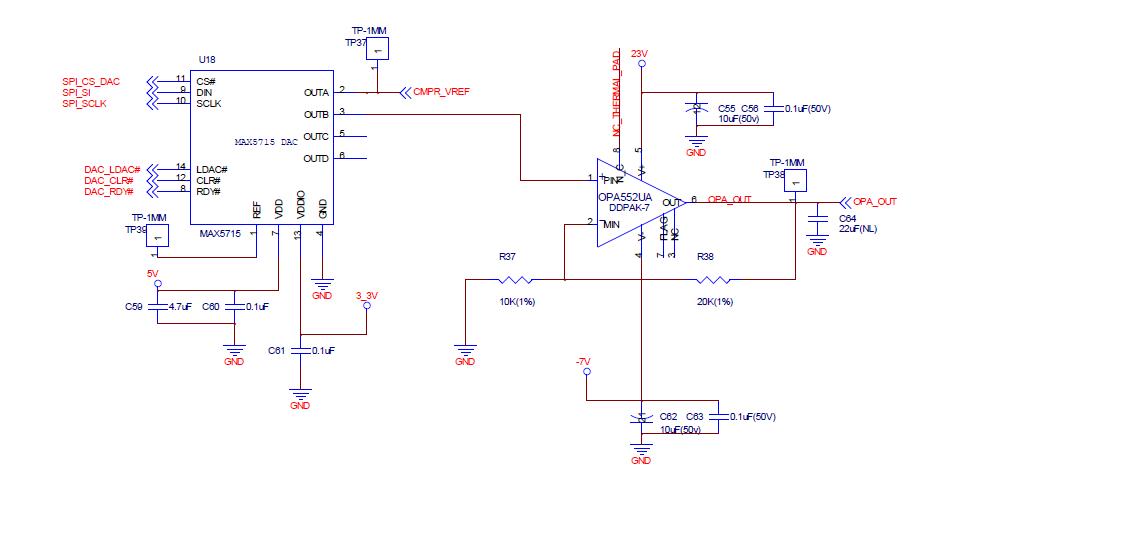
I have some OP amp stabilize issues in my design. I use DAC and OP amp in my system. And OP amp with a 22uF ceramic cap.

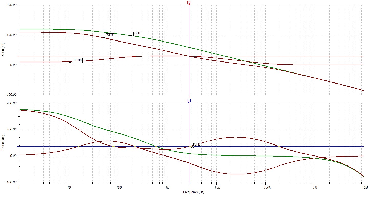
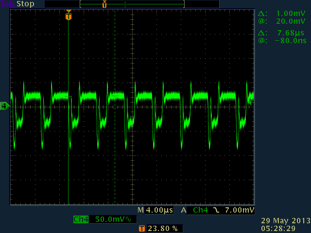
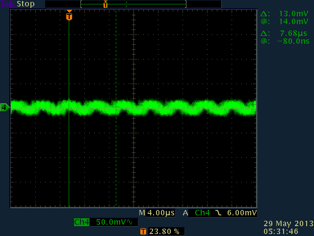
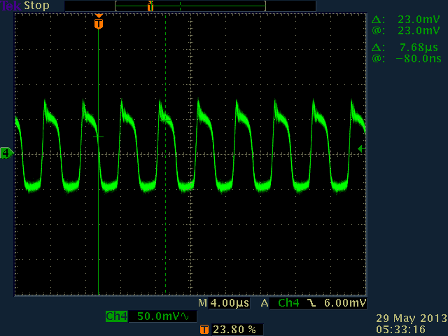
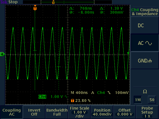
I use this op amp as non-inverting amplifier. And the schematic as attached pic. I found that Vout is oscillate and the current consume by OPA552 was very high(abt. 150mA).

I know that I can use OPA552 as Gain<5. Does this issues being solved if I change my op to OPA551? Or how do I stabilize this circuit? Thanks!

  • Dear all:

    If I can't change my design to OPA551. But I can change R38 to 40K ohm. let Acl = 5. How do I compensate this circuit if I still use OPA552. and Acl = 5. with 22uF cap load.

  • I will post the answer for this later today.

  • In general for Gains less than 5 use the OPA551 which is unity gain stable.  Due to your cap load and the new recommended compensation you can use OPA552.  See attached for new compensation for stability.  Inside the PowerPoint are embedded TINA SPICE files you can open and run with TI free SPICE simulator by link included in attached.  In addition I reference in attached an op amp stability article series that will give you all of the theory and techniques you need to understand this problem and future ones.

    OPA552 Cap Load Analysis.ppt
  • Dear Tim:

    Thanks for the solution! And Tina is really good tool.

    1.I'm a little confused about that the attached TSC file in your ppt page 6. I open this TSC file but there is no 22uF C-load and the Cf was replaced by 1nF; Rn replace by 634 ohm(compare to picture on page 6). And I try to fix this design to Cf = 100pF, Rn = 6.34k and add a 22uF C-load. is that right?

    2. I just wondering if I change my design to OPA551.Dose the compensation need to be modified or not?

    3. And I use TINA to simulate compensate just only Cf(because the PCB can't be modified as soon). The plot looks good and stable. But I add Cf(172pf) to my board in real world. The output of OPA still oscillate 172Khz and about 50mV. And It still consume about 150mA. Is that means I still have to add Rn Cn to my board? If it is true, why TINA simulation shows that will stable by just add Cf(172pF)? Thanks for kindly help.

    the attaches are the simulated result.0333.opa552_Cf.zip

  • See attached revised analysis for clarity and corrections. Sorry for the second pass as  I made a couple of mistakes.  In attached you will see a Loop Gain analysis of your experiment with the 172pF which shows loop gain phase dipping near zero and only 28 degrees of phase margin.  Your real world parts are probably not exactly the values you show in TINA so phase margin is probably less. Real world Aol will have variance from part to part as well.  Make sure you have 0.1uF bypass capacitors right at pins of OPA552 and within less than 1 inch at least 10uF of capacitance on each supply.   On any PCB you should be able to solder in recommended compensation parts on top of existing pads.  Note you will need to change feedback and input resistor values to 200k and 100k as shown in attached. If you change parts to OPA551 you will need to re-compensate with different values for stability.  You should consider soldering in recommended values in attached on your current PCB and check in lab. 

    OPA552 Cap Load Analysis Rev A.ppt
  • Dear Tim:

    Thank you very much! I really learned so many skills though I still need to digest these knowledge.

    And I'll try it in these days! Thank you anyway.

  • Dear Tim:

    I have a other question. Is the phase margin of the system defined by a. Aol intersect 1/beta or b. Vfb intersect 0db?

    I have seen so many definitions and the solutions you provide is Vfb intersect 0db. If I use Vfb intersect 1/beta. The phase margin of the system is 36 degree only.

    What's the difference between these definitions? Thanks.

  • You will find in the article series that the intersection of 1/Beta and Aol (what I call fcl)  is where loop gain goes to zero and the phase margin is looked at.  You can only look at phase margin by doing a loop gain plot.. Any relative phase of Aol or 1/Beta by themselves is meaningless for stability analysis.  To produce a loop gain plot one must break the closed loop open for AC loop gain analysis. This is why I use large inductor to keep loop closed at DC so SPICE can find a DC operating point before it can run an AC Analysis.  At any frequency of interest the inductor will look like an open.  Large cap couples in test signal since it is open for DC and short for any AC frequency of interest.   

  • Dear Tim:

    I modified my board to adding the compensation circuit Cf, Cn and Rn。

    And the output of the OPA552 seems stable.

    But It still consumes 110mA on 23V and -7V power source. And the OPA became very hot.

    And I measure the AC mode of the output as follows.

    And about +-15mV ripple still here@240kHz. I think that the reason why the OPA552 still consumes powers by charge and discharge C-load.

    I don't know the OPA is in stable or unstable state. If it's stable. Is that means I can only use the OPA552 with C-load and consumes such big power?

    Thanks for the kindly help!

  • We need to do some troubleshooting to discover the root cause of your high current draw.  With the sawtooth waveform you measure at 250kHz and 30mVpp ripple you can be consuming power.  Since Cload=22uF its impedance at 250kHz = 0.03ohms.  This voltage waveform on the output can cause high Iq.

    1) What power supplies are being used? Check power supply at op amp for ripple amplitude and frequency if any.  If power supply is a switching power supply the PSRR of OPA552 can allow power supply ripple across large cap load (22uF) causing high Iq.

    2) Remove 22uF capacitor and see if power supply ripple and amplitude changes.

    3) Does your PCB have both low frequency (10uF cap) and high frequency bypass (0.1uF cap) right at OPA552?  

    4) Is the low impedance output of the OPA552 routed anywhere near the +input of the OPA552?   

    5) is your oscillation shown in scope phots with DC output voltage and no other load than 22uF?

    6) Are you using DDPAK?  If so what is tab soldered to on PCB and what is that copper area connected to?

  • In addition do a closed loop stability test by injecting into the Power Op Amp circuit a +/-10mVpk signal at 1kHz into the input with the DAC disconnected.  Look at the output waveform for overshoot and ringing.

  • 1) What power supplies are being used? Check power supply at op amp for ripple amplitude and frequency if any.  If power supply is a switching power supply the PSRR of OPA552 can allow power supply ripple across large cap load (22uF) causing high Iq.

    There is really ripples at V+ and V-of OPA552. the V+ 23V plot as follows.

    And the very source of my power supply 23V is as phots.

    OPA -7 at OPA V-

    I'm using Programmable Linear DC Power Supplies and If there is no load for OPA. There is not ripples here.

    2) Remove 22uF capacitor and see if power supply ripple and amplitude changes.

    Yes there is still ripple if I remove C-load. and the amplitude of the ripple as photo.

    But there is not any ripple at 23V V+ and -7V -V at OPA552 pad. And of course There is no big current like before.

    And I found that, if there is no big current on the load, there is no ripple at power source.

    3) Does your PCB have both low frequency (10uF cap) and high frequency bypass (0.1uF cap) right at OPA552?  

    Yes. But the layout may be too far to the OPA. Please see attached layout photo.

    4) Is the low impedance output of the OPA552 routed anywhere near the +input of the OPA552?   

    No. there is not any impedance load.

    5) is your oscillation shown in scope phots with DC output voltage and no other load than 22uF?

    No. there is not any load beside the Cload 22uF.

    6) Are you using DDPAK?  If so what is tab soldered to on PCB and what is that copper area connected to?

    Yes. as phots.

    I think the suspect may be the de-couple cap. Here's the layout of my experimental board.

    The high freq. cap is too far for OPA552. But I'm not sure if it is the root cause of the problem I met.

    Do I need to use low ESR cap for 0.1uF and 10uF? even Cf and Cload?

    I use a normal ceramic cap and bulk cap. in this design.

    And Is there any remedy for the current version PCB?(increase the capacity of capacitor?)

  • From your last post:

    6) Copper area DD-PAK tab is soldered to is not connected to anything - correct?

    2) Removing Cload of 22uF will make OPA552 unstable since it was compensated only with 22uF present.

    I do have concerns about the routing of the high frequency bypass.  I will attach a recommended experiment to help get the high frequency bypass connected correctly.

    I also think for your application you will be better off with the OPA551 since you will not be using the bandwidth it even has based on compensation for a 22uF load.  What is your design with 22uF for?  A programmable power supply where you want a large capacitance out there for transient load conditions?

    If you switch to OPA551 let me know and I will recommend different compensation.  Also give me manufacturer's and part number and data sheet if you have it for 22uF load.  I am suspicious I may have missed a compensation issue if the capacitance is NOT ceramic. 


    OPA552 Cap Load Bypass experiment.ppt
  • Dear Tim:

    I really appreciate that you have the patience to help me solve the problem. Thank you!

    After I add the decouple 0.1uF cap. The AC waveform for V+/V- of OPA552 doesn't change. Output still ripple and and also the current still there.

    I use OPA552 with 22uF(murata GRM series ceramic) cap to be a kind of programmable power source. In my home-brewed flash memory test equipment.(flash usually need so many channel of high V).

    And for an other application I don't need the C-load cap. I just need it to be a Vref in flash memory.

    And just like you said I didn't need high bandwidth so OPA551 might be suit in this situation.

    Could  you help me to sompensate opa551 with and without c-load?


  • I assume you left 22uF cap on the output of the OPA552 when you tried the bypass capacitors directly on the output of OPA552.  One other remote possibility is to add a Snubber on the output of the OPA552 to ground, with 22uF cap load on and recommended new comp.  10 ohm and 10nF would be a good value to try.  I do not think this will make a difference but if it does let me know.  Also try replacing tour supplies with 9V battery for V+ and V- to see if oscillations go away.  I am a bit suspicious of your supplies still.  OPA551 is unity gain stable without any cap load.  For cap load I will send you recommended compensation. 

  • See attached for OPA551 with 22uF cap load.

    OPA551 Loop Gain.TSC