This thread has been locked.

If you have a related question, please click the "Ask a related question" button in the top right corner. The newly created question will be automatically linked to this question.

Problem with electret mic & INA217 - attenuation instead of gain

Other Parts Discussed in Thread: INA217, TL071

Hello everyone,


I'm having problems with the combination of the two.

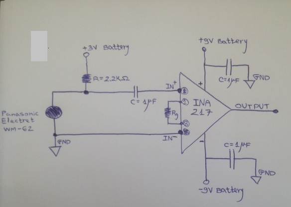
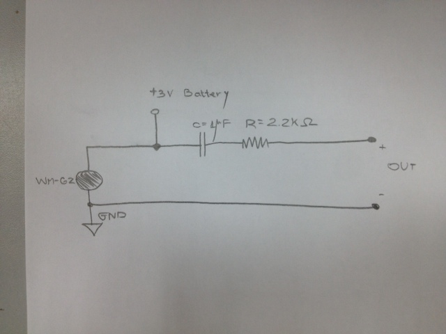
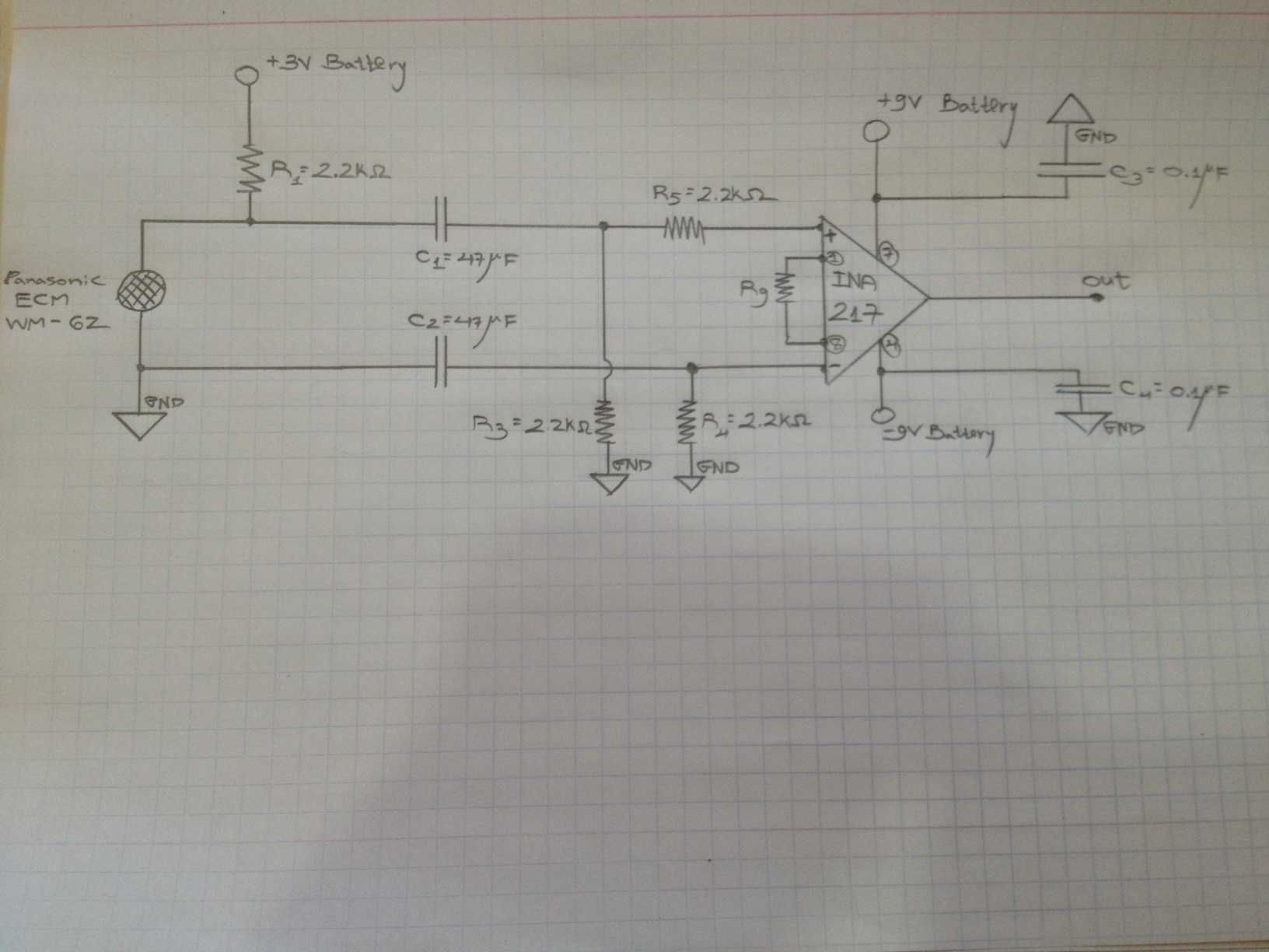
The electret mic is a Panasonic WM-62


My goal is to record audio speech at low frequencies ( up to about 4kHz ).

I'm using the schematics below to connect my electret mic to a Texas Instruments INA217 Instrumentation amplifier:


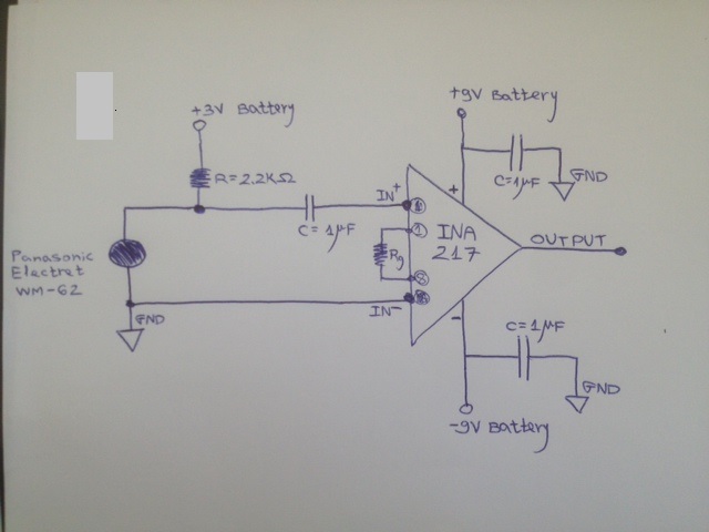
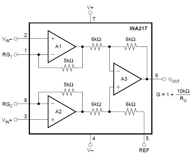
The gain equation for this amplifier is : GAIN = 1 + 10,000/Rg, where Rg is the value of the resistor between pins 1 & 8.

I tried to use all sorts of values for the gain. Theoretical gains of 50,100,200 all gave me a smaller peak to peak voltage while recording( attenuation! ).

I didn't have these problems when I connected the mic with a simple operational amplifier like the Texas Instruments TL071. With the 
TL071 I recieved very large gains at the output and it was very clean and good.


I have 2 questions:


1)What do you think is the problem with this circuit?
2)In general, are the bypass capacitor values O.K for frequencies as low as 4kHz? Should I use larger capacitance capacitors?

  • David,

    INA217 requires a DC input bias current of up to 12uA for proper operation (see PDS table below) that is NOT possible with your circuit configuration.

    Your input terminal, IN+, is AC coupled with C=1uF capacitor instead of being DC biased-this does NOT allow a DC bias current necessary for proper operation of the bipolar input transistor; in other words, R=2.2k resistor MUST be directly at the input of OPA217 (to the right instead of to the left of your 1uF capacitor) - see PDS application schematic below.

    Also, make sure to bias both inputs at the same DC level.  Since you use dual supply, +/-9V, most likely both inputs should be biased at 0V with a use of two resistors (R4 and R5) as shown in the schematic below; biasing IN+ at 3V while IN- at 0V with a close-loop gain of 3 or greater would result in the output collapsing on one of its rails.

  • Thank you very much Marek,

    If you don't mind, I have a couple of follow up questions:

    1)In Panasonic's PDF about electret mic's, the schematics is:

    You suggested putting the R=2.2k ti the right of the C=1uF. Did you mean I have to replace the existing R=2.2k? Or should I just put an additional R=2.2k to the right?

    2) I'm trying to understand why putting a resistor to the right of the capacitor will force a DC current on this path. I'm clearly missing something. To my best knowledge,

    as long as there is a capacitor on this path, DC current should NOT flow.

    3)I'm working with very low frequencies ( infrasonic freq. too ). Should I change the value of the capacitors to a higher capacitance? 

    Again, Thank you for your explanations,

    David.

  • David,

    Please see my comments below:

    1)In Panasonic's PDF about electret mic's, the schematics is:

    You suggested putting the R=2.2k ti the right of the C=1uF. Did you mean I have to replace the existing R=2.2k? Or should I just put an additional R=2.2k to the right?

    The Panasonic's schematic above is highly simplified and does NOT provide the biasing details necessary for proper operation of any instrumentation amplifier.

    The R=2.2k resistor at the input of your circuit (see below) does NOT do anything other than loading WM-62 signal source so it should be eliminated and replaced with the resistor right at the IN+ input.

    2) I'm trying to understand why putting a resistor to the right of the capacitor will force a DC current on this path. I'm clearly missing something. To my best knowledge,

    as long as there is a capacitor on this path, DC current should NOT flow.

    There will be a typical IB current flow of 2uA (maximum 12uA) at IN+ and IN- input terminals with or without input decoupling capacitor.  Without IB INA217 would not work at all since IB is nothing else but a base current necessary for normal operation of the pnp input transistors.

    The difference is that with a decoupling capacitor the input bias current will continue charging the input capacitor, Vcap = 1/C*∫ i*dt, until IN+ reaches one its rail (and output saturates against its rail) while by using a resistor input current will result in a fixed change of the input offset: Vos=Vos_initial+IB*RB (typical Vos_change=2.2k*2uA=4.4mV) - however, by placing resistors on both of the input, as shown below, you will minimized the Vos change by a typical: Ios*RB (0.1uA*2.2K=220uV).


    3)I'm working with very low frequencies ( infrasonic freq. too ). Should I change the value of the capacitors to a higher capacitance?

    Since the actual input voltage directly at the IN+ input terminal is a function of the ratio of the input impedance: VG1*R4/(R4+Zc1), maximizing the size of decoupling capacitors will minimize the attenuation of the input signal; therefore, it would be a good idea to make C1 and C2 as large as possible especially in case of low frequency signal.

  • First of all, thank you for your answer.

    I'm having problems with leaving the R=2.2k out of the path from the 3V battery to the mic.

    The schematics now is:

    When I measure the output voltage, all I see is noise. The mic isn't responding.

    What is the cause?

    David.

  • I've connected the following circuit and it simply doesn't work:

    I also see strange oscillations at the output.

  • David,

    First, in order for your circuit to work you may NOT float REF pin 5 - see below.

    REF pin must be connected preferably to GND (see below) - I do not see it at all on your schematic.

    Also, there is no need for R5 resistor shown in your circuit - it only increases the input voltage offset between the input terminals.

  • Thank you for your replies, Marek.

    I've managed to make the circuit work after your advice.

    The circuit is now:

    The circuit works with all kinds of values for Rg and gains.

    But I still have 2 problems:

    1. I have a voltage offset of minus 5mV at the input, when the INA217 is connected to power. This of course corresponds to a greater voltage offset at the output (offset input*gain)

    2.Every time I connect the 0.1uF capacitors from the power sources to ground, The INA217 begins to oscillate and heat up very rapidly.