This thread has been locked.

If you have a related question, please click the "Ask a related question" button in the top right corner. The newly created question will be automatically linked to this question.

Switched Integrator ACF2101 spectrum analyzer

Other Parts Discussed in Thread: OPA4131, ACF2101, OPA2107

Hello,

I had a few questions about the spectrum I'm measuring at the output of my buffer circuit with the switched integrator, an ACF2101.  The buffer amplifier is the OPA4131.

http://www.ti.com/product/acf2101

http://www.ti.com/product/opa4131

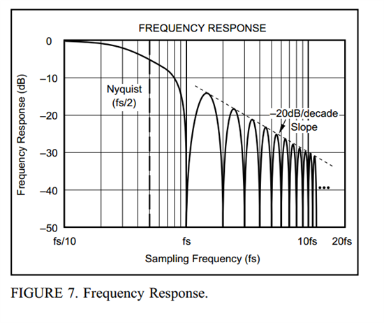
The datasheet shows the frequency response for a ACF2101 below.  I agree, fourier spectrum of a rectangular pulse is a sinc function with null at the sampling frequency and all harmonics.  

The timing signals I generate are the same as presented in Figure 9 of the ACF2101 datasheet.  I use a microcontroller to generate the signals with a PWM or software timed.  It's periodic with sampling frequency fs.  

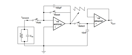
The circuit is the same as below, just the OPA2107 has been replaced by the OPA4131.  The input network i s a photodiode with shunt resistance 500 Megaohm and shunt capacitance 10 pF.  No reverse bias applied.  A 10 nF poly cap is for S/H operation.  No external cap for ACF2101, just the internal 100 pF.

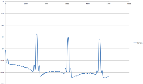
I ran simple experiment where I set the hold time to roughly 600 usec.  The select and reset were set to 30 usec, so the entire integration period is ~660 usec.  I was expecting a clean output like the datasheet, instead I get the following for my spectrum analyzer response in a bandwidth of 5 kHz.  The first null should be around 1/660usec or 1.515 kHz so thats pretty spot on.  But there are big tones at every sinc NULL spot. 

I do not understand this response so I'm requesting some help.  What exactly am I seeing here?  I don't believe this is a grounding error.  I will post back when I pull the photodiode and try 1) grounding input and 2) putting in a current source.  The instrument noise floor is clean too in this bandwidth with no spurs down to -127 or so.  The instrument used for analysis is a HP 3561A dynamic signal analyzer.

  • Hi John,

    I am working my way through a backlog of inquiries - sorry for the delayed response. Let me look over your information carefully and have a chance to give it some thought.

    Regards, Thomas

    PA - Linear Applications Engineering

  • John,

    I trust that you are measuring the spectrum at the output of the sample/hold circuit, not directly at the output of the AFC2101. In the possible case that you are measuring at the output of the AFC2101 and for others who might be curious, I'll provide this explanation:

    The purpose of a switched integrator is to measure the voltage at the end of the integration period. An input signal with a period equal to the integration period will have zero value at the end of the integration. During the integration period, however, you would see an output waveform that has substantial variation at the input frequency.

    So a continuous spectral analysis of the output voltage throughout the integration period will certainly not produce the expected sinc function spectral response. You will see plenty of the input frequency, regardless of its relationship to the integration period. To see the expected response, you would sample the output at the end of the integration period.

    Assuming that you are measuring at the output of the sample/hold circuit (the additional op amp) there are a couple of possible reasons for spectral content at 1/T, the integration period:

    The internal integrator op amp has a very limited positive output voltage swing above ground--approximately 0.7V. If your test signal with period 1/T is too large, you may be overloading the integrator op amp. Check the output voltage swing during integration. It should not exceed +0.5V, or so.

    Another possible cause would involve the timing of the select switch on the output of the ACF2101. This switch should only be on during the integrator hold period. Any timing overlap prior to the start or after the end of the hold period will cause a glitch in the output of the sample/hold. Some guard band may be required in the timing to avoid overlap. Mistiming of this switch would significantly alter the spectrum. Check the time-domain waveform at the output of the sample/hold for evidence of any improper timing.

     Hope all this is clear.

     Regards, Bruce.


  • Bruce,

    Thanks for your response.  I've continued work on this problem and am seeking additional help.

    First, I want to explain my purpose here.  I'm looking to make a noise comparison between a conventional trans-impedance and integrator front-end.  Theory states that a larger integration time results in a smaller equivalent noise bandwidth and hence a smaller noise contribution.  To this point, I've successfully matched theory and measurements for the noise floor of a transimpedance amplifier with the stated photodiode inserted at the input.  The question I'm trying to answer is how many dB do I drive the noise floor down by using the switched integrator with larger integration times.

    1. I agree, if I inject a test current sinusoid of the inverse frequency of the integrator then I would expect no DC output.  Any charge integrated from the high side would be cancelled by the low cycle.  I could reason that the fundamental and harmonic frequencies would show up.

    2a. I don't believe its overloading as the DC output never approaches 0.7 Volt.  I have inserted the photodiode and covered it completely by enclosing it in a rubber black grommet.  Therefore, there is no photocurrent and the DC output is near the system GND (0 Volts).  I don't want a fixed DC current because that would limit my ability to integrate for long times (the largest I want to go is 1 second right now).  

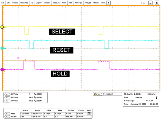
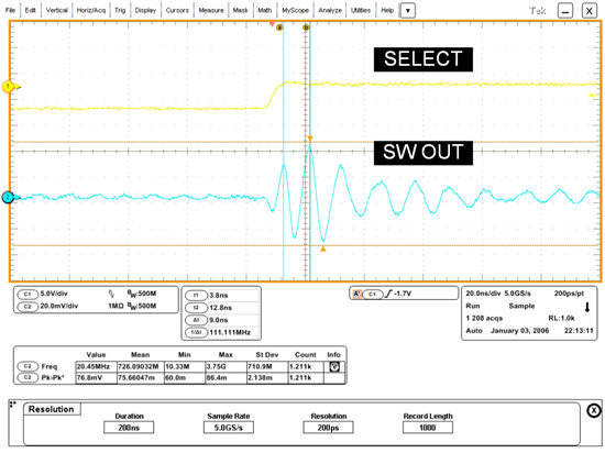
    2b. I don't believe it's a clock timing issue.  I'm generating these clocks from a MCU in firmware so theres a substantial delay between hold, reset, and select clocks.  A tex oscilliscope capture of my clock is shown below:

    I worked with my advisors on this and found that there is a high frequency ripple after the S/H output.  My actual implementation waits a certain time (say 100 usec) before the AD samples the output.  However, the problem was when I ran the HP 3561A in free-run mode it captures this high frequency ripple.  I think the origin of the ripple is from the capacitive divider formed from the parasitic of the Select FET internal to ACF2101 integrator.

    I have other ideas for how to make this measurement.  I've tried to manually trigger the HP 3561a a certain time (100 usec) after the ripple.

  • I wanted to separate my previous response with this one for the purpose of identifying new procedure for this measurement.

    My goal is to vary the integration time for 100 usec, 1 msec, 10 msec, 100 msec, and 1 second to show that the noise floor falls for the longer I integrate.  Burr Brown doesn't give a specification for the noise spectral density of the amplifier but they do say that from 0.1 to 10 Hz is 2 uV rms so this is presumably the 1/f region. 

    The switched integrator acts like a low pass filter and the equivalent noise bandwidth is proportional to 1/T.  If I could omit the flicker contribution and the noise was white than I would expect the RMS noise to decrease by 20*log10(sqrt(1/10)) = -10 dB for each decade increase in integration time.  However, the noise being flicker I should expect more noise contribution for the longer I integrate.

    1. Can anyone recommend the procedure or process they would use to measure this?  I've capture oscilliscope time waveforms for each integration time (100 usec, 1 msec, 10 msec, 100 msec, 1 sec) and brought the data into MATLAB.  I manually remove the high frequency ripple from the switching operating and have taken the RMS using the standard deviation.  The standard deviation decreases for integration time but not in a discernible pattern.  In fact, the 1 sec integration time actually is larger than the 100 msec result.

    My understanding of flicker noise is poor as its kind of a esoteric topic.

    2. In reality I want to measure this with the Signal Analyzer (spectrum analyzer).  I did an experiment where I manually triggered the analyzer 100 usec after this ripple.  When I did this, I set the span to 100 kHz expecting that the LPF action of the integrator would attenuate the HF noise above the integrators NULL frequency.  The spectrum with a span from DC to 100 kHz for different integration times (100 usec, 1 msec, 10 msec, etc.) are all the same and i don't see any LPF action.

    3. Should I sample during the S/H operation (ie: when the Select switch is closed) or should I sample the charge held on the S/H capacitor?  My scope captures look the same in magnitude for both cases so I took them from the capacitor.

    I very much appreciate any help and feedback.  Apologies on taking a while to respond, been working on several matters but really need to get to the root of this problem

  • John,

    You've asked many thought provoking questions that gave me some sleepless hours last night. Be aware that I'm now retired and thus have the privilege of offering opinions and guesses without validation or guilt. :-)  So here are some opinions and guesses...

    With no current input to the integrator, I see two main contributors to noise:  1)  Voltage noise of the op amp is passed to the output at nearly G=1 in your case.  2) the sampled capacitor noise when the reset switch is opened.

    Neither of these noise sources is integrated so they are not subject to the sinc transfer function. The sinc frequency response applies only to currents integrated on the capacitor. This would include any input signal current noise and input bias current noise. I believe that these are virtually zero in your test case.

    The output S/H circuit also adds noise. As you indicated, you can probably eliminate this stage and sample with your instrumentation on the fly.

    In your MatLab standard deviation calculations be sure that you are removing the DC value by subtracting the average of all data points from each datum.

    You are certainly working into the 1/f region of the integrator op amp. The ACF2101 was designed for a specific customer application about 22 years ago and was never fully characterized as a truly general purpose device. So there are likely no data available for many of the characteristics that might interest you.

    Here are links to a few blogs that you may find helpful. In particular, the last one on 1/f noise will give you a jump-start on this type of noise:

    Resistor Noise—reviewing basics, plus a Fun Quiz

    Op Amp Noise—the non-inverting amplifier

    Op Amp Noise—but what about the feedback resistors?

    1/f Noise—the flickering candle

    I hope this is helpful,

    Bruce