


The embedded systems including 1 ADC,1 Vref,2 DAC,4 Amp。the ADC is ∑-△ type,so its high speed.i need a very Clean ground plane.how should i place them?
1、star nood:i means i must Gather all the connections to a node Physically?
2、Supply rail and gnd rail:like this:
How to arrange these devices Now?
a,An argument said that:IC.NO.1 is should place the Most vulnerable to interference。the reason is No.1.IC should have the Nearest to ground loops。(Assuming the power chip is on the left)
b,anohter argument said that:Maximum Number IC should be place the Most vulnerable to interference.because this ic may Minimal interference received。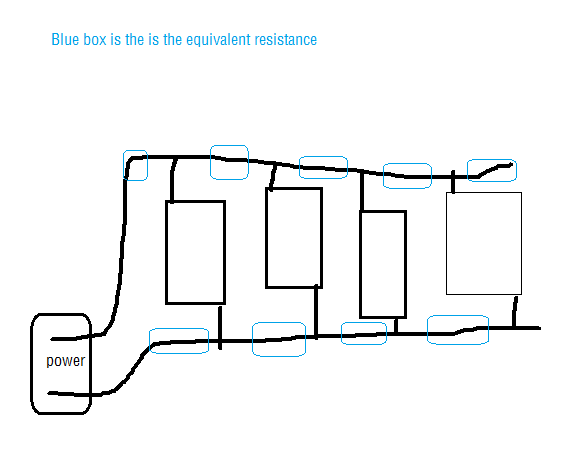
a:Supports A view of people think that :1 device has a minimum of the resistance to ground
b: think that:if the right side device is the ADC or MCU,so the Current fluctuations may All of the devices through the influence(all the device on its left side )so the ADC or MCU should place the more left the better.
Now,Will you engineers, which of these three is the correct view, and explain the reasons??thanks!!