This thread has been locked.
If you have a related question, please click the "Ask a related question" button in the top right corner. The newly created question will be automatically linked to this question.
Hello TI engineers
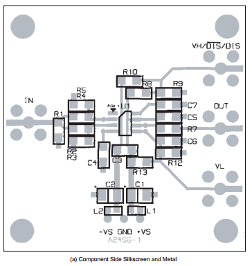
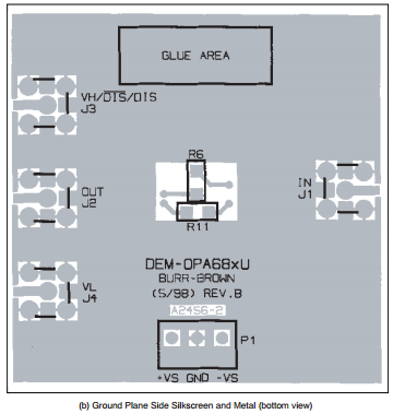
I saw PCB for high speed amplifier DEM-OPA-SO-1A like a picture and I have 2 questions about this design.
1. Why top side has no ground plane?
2. Why ground plane at bottom side blank area IC ?
Best regards
Witat
Hello Witat,
I can't answer for the missing ground plane on the top layer, but the cut out from under the amplifier is to reduce parasitic capacitance on the I/O pins. The inverting input and the output pins are both sensitive to parasitic capacitance. This is explained on page 5 of the datasheet.
This looks like an older design. We don't use many through hole SMA connectors anymore. Edge mounted connectors provide a better impedance match.
Loren