This thread has been locked.

If you have a related question, please click the "Ask a related question" button in the top right corner. The newly created question will be automatically linked to this question.

Common Mode Error of Fully Differential Amplifier (LMH6552)

Other Parts Discussed in Thread: LMH6552

Hi,

Regarding the usage of LMH6552 as ADC driver, similar to fig. 50 and 52 in the datasheet.
What should taken into consideration in order to estimate the deviation of the common mode voltage at LMH6552 outputs from Vref?
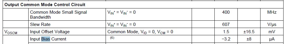
In particular, what is the meaning of the following parameters: "Input Offset Voltage", "Input Bias Current","Input Resistance" and how should they be used to calculate the CM error?

Thanks.

  • Hi David,

    • The "Input Offset Voltage" (VOSCM) found under "Output Common Mode Control Circuit" section refers to what the measured output CM voltage {("+OUT" + "-OUT") / 2} is when the differential input (VID) is 0 (e.g. VS in Figure 46 set to 0V) and both device input pins (+IN and -IN) are at mid-rail (0V with V+ = 5V, and V- = -5V):


    The measured out CM voltage could be as large as +/-16.5mV.

    Note that the CM control circuit gain is ~1V/V. So, measured output CM offset is equivalent to the offset voltage at the VCM pin.

    • "Input Resistance" (15ohm differential) is the resistance looking across the inputs (+IN and -IN). "Input Resistance" (under CM control circuit) (200kOhm) is the impedance looking into the VCM input. For your purposes and the CM output offset, you need not worry about either of these parameters, especially if you are driving the VCM from a low impedance voltage source.


    • "Input Bias Current" (IBI) is the current that flows into each input (+IN and -IN). As long as RF values are matched, this current causes no output differential output offset voltage. The CM control loop keeps the output CM offset to the limit (VOSCM) mentioned above.


    Regards,

    Hooman

  • Hi Hooman,

    Thank you for your reply.

    Some follow up questions:

    1. By "Input Bias Current" I meant the one that is mentioned in "Output Common Mode Control Circuit" section. Is this current flowing in/out of the Vcm pin? If yes, in a case that there is some series resistance between the Vref of the ADC and Vcm of the LMH6552 (or in a case of Vref output having relatively high impedance), will it develop voltage drop on that resistor and by that contribute to the common mode error?

    2.  My goal is to gather all possible factors that may contribute to common mode voltage error, i.e. the deference between the  voltage measured on Vref pin and the output CM voltage {("+OUT" + "-OUT") / 2}. Below is a list of these factors as per my current understanding. Could you please confirm that list and correct/complete if required?
      1. "Input Offset Voltage" (VOSCM).  Max contribution: 16.5mV.
      2. Gain (ΔVO,CM/ΔVCM). Max contribution: (1.012-1)*Vcm , i.e. for Vcm=1V, will contribute 12mV to the error.
      3. (?) Input Bias Current (page5). Max contribution: 8uA*Zout_Vref.
      4. (?) Voltage divider between the output impedance of the Vref pin and the "Input Resistance" (200kOhm).
      5. Anything else?

    Regards,

    David.

  • Hi David,

    You are correct about "Input Bias Current" in the "Output CM Control Circuit" section. It refers to current flow into the VCM pin. Yes, any drop in the Vref series resistance will affect the VCM pin voltage and hence the output CM:

    Regarding your specific questions:

    a. VOSCM: Agreed

    b. Gain (1.012V/V max): Not totally agreed. The CM control loop looks at OUT+ and OUT- and makes their average / CM value within +/-16.5mV of the VCM pin voltage. So, in my opinion, there is no additional error due to Gain not being exactly 1V/V.

    c. VCM Input Bias Current into Vref pin impedance: Agreed

    d. Voltage Divider on VCM pin: To me, this is the same as "c" above where you get a voltage offset due to current flow into the VCM pin through the Thevenin equivalent of whatever is between Vref and VCM pin

    e. Anything Else?

    "Output Balance Error" (-60dB) corresponds to the CM output that appears for a given differential output swing. So, if the diff output is 2V, you would expect a CM output of 2mV (based on the -60dB rating)


    Regards,

    Hooman