


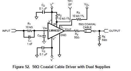
I've got an LMH6321 design which worked fine in the previous version but is now failing in an odd way. I'm attaching a schematic sketch which shows the two versions, working and not working. The symptoms are that the current limit pin (CL) is pulling to +15 V instead of staying at virtual ground, and the output is slightly unstable at high levels.
>
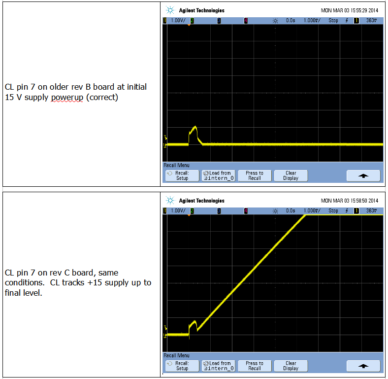
The main problem seems to be CL pin pulling high. If I lay a finger on CL the instability goes away, and there is a distinct difference between the old circuit CL (at ground potential as it ought to be) and the new CL (at +15 V).
>
The input to the LMH6321 is identical for both versions, and I've added a couple of (what I thought were) harmless things on the output which has caused the problem. The main difference is AC coupling on the output, but I have tried shorting the 10u AC coupler and that doesn't help. I've also tried removing the 38.3k pullup AND shorting the 10u AC coupler, and I've tried putting a 50 ohm load to ground with all that in place. Nothing makes the CL (pin 7) go to ground potential as it should.
>
I've checked all the supplies and connections to the LMH6321, all the passive component values in the circuit, and even replaced the LMH6321 itself. The problem remains. If I power up an old (working) board (with no signal input) the CL pin is at ground potential as it ought to be, and if I power up a new one (doesn't work) CL is at 15 V and the output shows the slight instability when I apply a large signal.
>
The PCB layout between the two versions is almost identical, too, especially for the power and decoupler connections. It's not shown on the sketch, but the power tab is connected to -15V.
>
I contacted TI support ten days ago with this problem, emailed three times and called again, only to be told this morning they are moving all support to this forum. This is certainly aggravating and my client is getting impatient. Can anyone shed some light on this problem?
>
Thanks,
Gerrit

