This thread has been locked.

If you have a related question, please click the "Ask a related question" button in the top right corner. The newly created question will be automatically linked to this question.

AMC1100 input protection

Other Parts Discussed in Thread: AMC1100, LMV601, OPA350

Dear Mr Jose Duenas Cuellar!

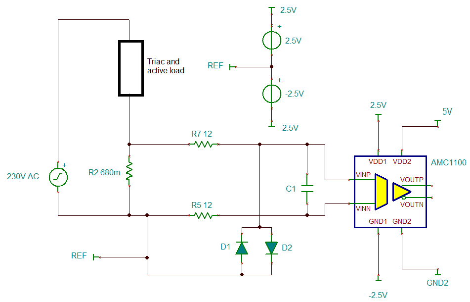
I thought about circuit in the attached Figure 4  (with TVS or Zener diodes)

Voltage at the R2 resistor may be 10-12 V in overcurrent moment. If to use Zener diodes, then if current flows in I2 direction, then at VD2, VD3 will be voltage 3V and at VINP, VINN will be voltage 3V relatively GND1.

If current flows in I1 direction, voltage applied to VD2, VD3 in the forward direction, then voltage at VD2, VD3 will be 0.7V and VINP, VINN will be 0.7V negative relative GND1. But max negative voltage at VINP, VINN must be no more than 0.5V.

Please, answer 

1) Is it essential that this negative value will be 0.7V i.e. more than 0.5V?

2) Can we use R8 in order to decrease input voltage, if max voltage at the R2 is more than 250 mV?

Please,

TIA

Vladimir Naumenkov  www.agat.by

Figure 5_02.04.2014.docx
  • Dear Vladimir Naumenkov,

    After reviewing the new schematics you sent I see your point. With regard to your questions:

    “1) Is it essential that this negative value will be 0.7V i.e. more than 0.5V?”

    Answer. It is essential that:

    a)      the voltage on pin 2 of the AMC1100 never rises more than 0.5 V above the voltage present on pin 1.

    b)      the voltage on pin 3 of the AMC1100 never rises more than 0.5 V above the voltage present on pin 1.

    c)       the voltage on pin 2 of the AMC1100 never falls more than 0.5 V below the voltage present on pin 4.

    d)      the voltage on pin 3 of the AMC1100 never falls more than 0.5 V below the voltage present on pin 4.

    Accomplishing c) and d) is going to be very difficult with the schematic you have proposed.

    “2) Can we use R8 in order to decrease input voltage, if max voltage at the R2 is more than 250 mV?”

    Answer. You can use the combination of R5, R7 and R8 to divide the voltage drop on R2 but they do not solve the problem of over-voltage on the AMC1100 input. Also, R8 will change the cut-off frequency of the filter provided by R5, R7 and C1. The major issue with using R5 and R7 is that 75 ohms can potentially cause settling issues in the internal input sampling capacitor of the AMC1100. My recommendation would be to use values for R5 and R7 below 20 ohms to prevent such settling issues.


    To prevent the AMC1100 from being damaged during a short circuit event, I would recommend using a circuit similar to the one below.

    Note that it requires two 2.5 V supplies connected to the node labeled “REF”.

    Assuming that the short circuit event produces about 14.7 A at maximum (10 V / 0.68 ohm), the diodes D1 and D2 could be selected to be similar to the BAV99.


    For that scenario, in the event of a short circuit the diodes would shunt about 0.7 A with around 1.35 V of forward voltage. Such forward voltage added to the voltage drop on R5 or R7 (depending on the direction of the current) will produce a combined voltage equivalent to the voltage drop caused by the remaining current flowing through R2. If the short circuit current can be significantly higher, then I would recommend adding the bi-directional 6.8V TVS diode labeled VD1 in your schematic with the caveat that it needs to be connected directly in parallel to R2 (otherwise the series R4 will make VD1 completely ineffective).

    Two potential problems of using diodes to clamp the positive input terminal are: 1) forward current of the diode during normal operation of the AMC1100, and 2) mismatch in the common-mode capacitance introduced by the diode. The system will work properly as long as both the forward current at 250 mV and the parasitic capacitance of the diode are small. For example, a diode similar to the BAV99 should not cause problems since its forward current is less than 2 uA at 250 mV (2 uA is much smaller than the expected full range current of 367.6 mA). The parasitic capacitance of the BAV99 is less than 1.2 pF, the mismatch in common mode capacitance will not affect the system as long as C1 is much larger than 1.2 pF.

    Hope this helps.

    Best regards,

    Jose

  • Dear Mr. Jose Duenas Cuellar!

    Thank you for your answer. Please, see the attach. Could you, please, recommend inexpensive operational amplifier for DA2?

    TIA

    Sincerely

    Vladimir Naumenkov  www.agat.by

    Figure 6_03.04.2014.docx
  • Dear Vladimir Naumenkov,

    Do you have a general idea of the approximate capacitive load connected to the output of DA2? Such load would be the parasitic capacitance between the GND1 and the lower node of R2.

    If the capacitive load is relatively small, then something like the LMV601 should suffice. If the capacitive load is significant, then somehting like the OPA350 will be needed.

    Best regards,

    Jose

  • Dear Mr. Jose Duenas Cuellar!

    Thank you.

    Sincerely,

    Vladimir Naumenkov  www.agat.by