This thread has been locked.

If you have a related question, please click the "Ask a related question" button in the top right corner. The newly created question will be automatically linked to this question.

OPA376DCK INPUT OFFSET VOTLAGE

Other Parts Discussed in Thread: OPA376

We use OPA376AIDCK as PCB trace current sense amplifier; the diagram is like below; we tried several samples and found some of them show very large equivalent input offset voltage under high working temperature like between 100'c and 125'c; the equivalent input offset voltage could be as high as 3mV(the higher the working temperature, the larger the equivalent input offset voltage)!!!  while with working temperature below 100'c, the equivalent input offset voltage is very low; We did the test with DC input signal  VS1=-6mV and no OSC was found on output by the way;

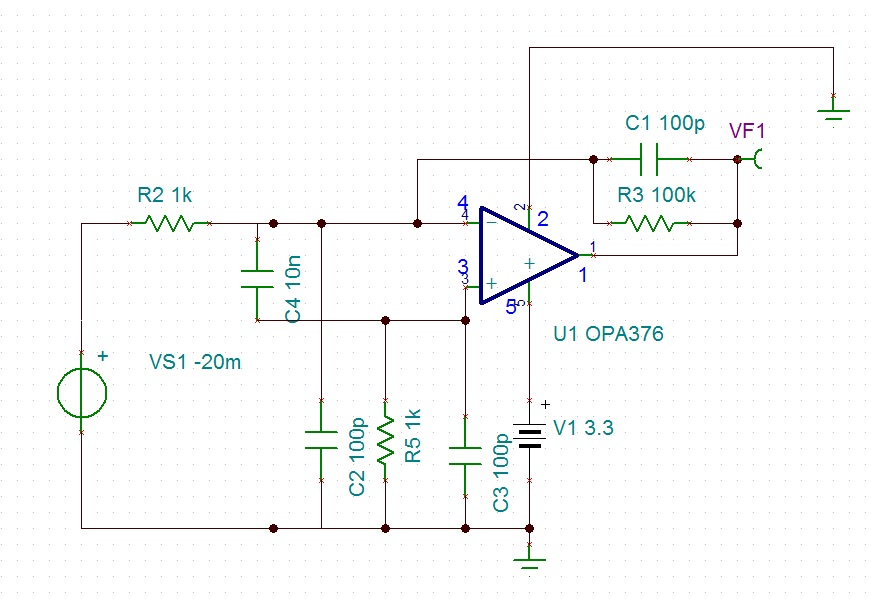
According to OPA376AIDCK's datasheet, the total equivalent offset voltage over Vsupply, working temperature range(25'c-125'c) and Vcm should be less than 0.3mV; while the test result is really bad for some samples; 

  • update some test results; 

    Input signal -7mV, output is around 0.35V; for bad sample and good sample, they're all tested under the same test condition: Remove C4 doesn't help;

  • Sorry, the good sample test data in chart of output voltage vs working temperature should be of bad one, the bad sample is for good one; 

  • Jun,

    The input bias current doubles every 10 deg C, so the maximum IB of 10pA specified at 25 deg C may result in IB=10nA at 125 deg C (10pA*2^10) -  see a typical graph below.

    Therefore, I suspect that the reason behind the Vout becoming non-linear in your application is the increase in IB current at high temperature - please replace R5 with a short (it is NOT needed for CMOS input amplifiers) and see if this will solve your problem.  BTW, placing C4 of 10nF between the input terminals may result in the current leakage as well as cause instability of the circuit configuration-please remove it unless it is used for continuous low-pass roll-off.  

  • Marek:

    IB*R5=10uV which  is very small compared to 1100uV;  and we have tried to remove C4 and short R5, the problem is still there;

    we tried 6 samples and 3 of them shew very bad equivalent input offset voltage when working temperature above 90'c; 

    We want to know what's the maximum possible output error it could be over the whole working temperature range of OPA376;

  • Jun,

    Your circuit above shows the close-loop gain of G=-100 but your description (Vin=-7mV, Vout=350mV) suggests your actual gain is G= -50.  Could you please provide the schematic used in taking the data including the actual value of R2, R3 and R5 resistor?  BTW, you must also use at least 0.1uF bypass capacitor between VDD and ground - not shown on your schematic.

    The OPA376 maximum input voltage offset at 25 deg C is specified to be +/-25uV while the max drift is +/-2uV/C (see below) so these could result in the maximum Vos of +/-225uV at 125C - far less than 1100uV you claim to see.  If you actually use supply bypass cap and made absolutely sure the part is stable, the only other cause I can think of for the excessive offset voltage would be ESD or EOS damage; if you wish to confirm it, you would need to contact your part supplier to arrange the return of the suspect units for failure analysis.   

  • Marek:

    Sorry, R3 in first diagram should be 49.9K and this diagram was drew in TINA so the LDO power supply and bypass cap are not shown;

    We would arrange the failure analysis according to your suggestion; thanks a lot;

    Jun Yin