Because of the holidays, TI E2E™ design support forum responses will be delayed from Dec. 25 through Jan. 2. Thank you for your patience.

This thread has been locked.

If you have a related question, please click the "Ask a related question" button in the top right corner. The newly created question will be automatically linked to this question.

INA331 Output noise when using amplification configuration via external resistors

Other Parts Discussed in Thread: INA331, TLC272, INA146, TINA-TI, TIPD101

Hi all,


we are using a INA331 in an electrical measurement device. The INA331 is used to condition the input signal for ADC input with a total output range of 0-2.38V having 1.19V as reference and zero point.

The voltages to be measured (between P5 and P6) are from -4.6V to +4.6V, AC (20-400Hz) or DC.

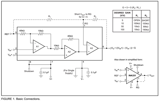
The following problem occurs: when using external resistors for setting the gain (see basic connections drawing R1 and R2) the INA has a high output noise of about 50mV which means 2% of output range! The noise is independent from the gain level and even occurs at the default gain level of 5.

When the fixed gain of 5 is used by setting R1 to open and R2 to short, the noise is completely gone.

The noise seems not to be coming from the reference side, because when R1 is open and R2 is at 110k, the noise also occurs.

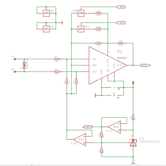
In our application, the gain level shall be switched via a 4066 switch by setting different values at R1, having 3 levels of gain.

Please see our schematic. Gain configuration is done by R14 and R15 (for fixed gain) as well as R26 and R27 (alternatively, switched by the 4066 switch IC8)

Thanks for any help!

Christian

  • Hello Christian,

    First, have you looked at the input pins, supply voltage, and reference voltage pins on an o-scope?  If so, can you please post the waveforms?

    From here I recommend isolating and testing the INA331 by doing the following:

    1) Remove R1, R2, R7, and TLC272
    2) Replace R3 and R4 with 0ohm resistors.
    3) Apply 5V to pins 7 & 8
    4) Apply 2.5V to inputs (pins 2 & 3) and reference (pin 5)
    5) Set the device in a gain of 100V/V (remove R26 and R27, replace R15 and R14 with 10kohm and 190kohm resistors, respectively). You can then adjust the gain to see if you observe the same behavior as before.

    Finally, are you using 55V to switch IC8A?  I expect this should be 5V5.

    Please let me know the results!

  • Hi Pete,

    thanks for the reply.

    First of all the IC8 is switched by VDD (3.3V), 5V5 and 55V are just the names of the outputs.

    I will be trying to set up your test scenario and post the results.

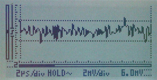
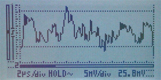
    I got two boards, one with the 110k resistor at R14 and one with 0 ohm at R14, this is what it looks like on the oscilloscope. It seems that the noise is still there, but with reduced amplitude. Maybe factor 5.

    Please have a look (110k version)

    _

    and the verson with zero ohms

  • Hi Pete,

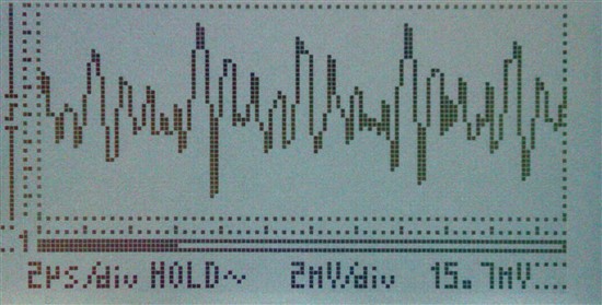
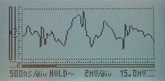
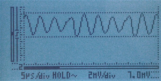
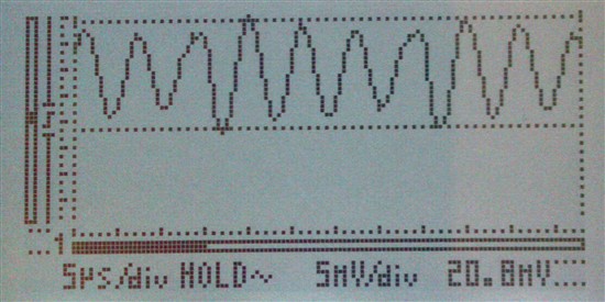
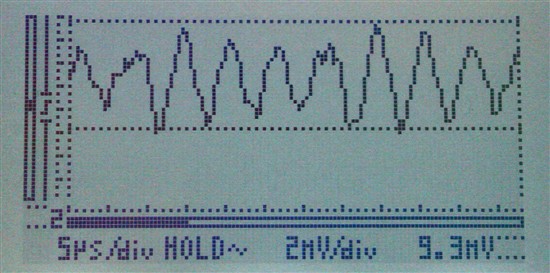
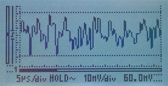
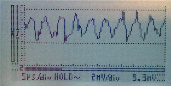
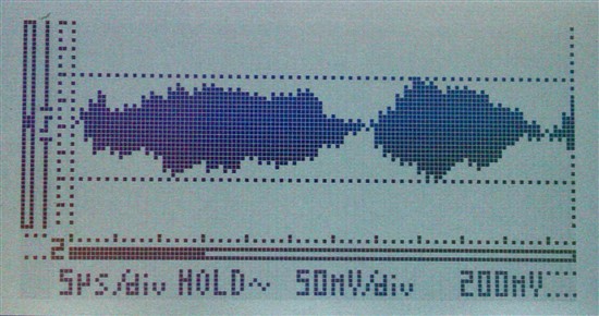
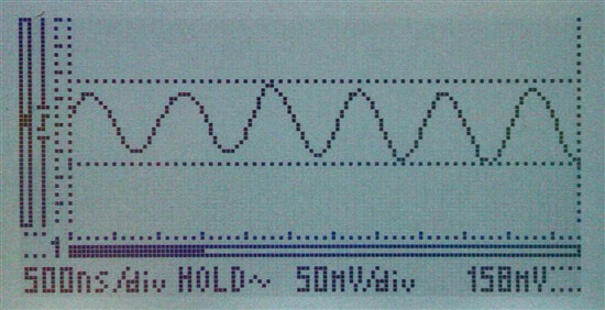
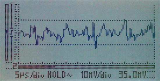
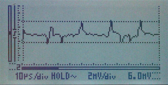
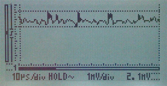
    i made some more measurements, please have a look at the result. In the lower right corner is the peak-to-peak voltage (distance of the the dotted lines).

    Measurement with on-pcb power supply

    Signal at the input pins

    Signal at the supply of the amp

    Signal at the reference

    Signal at the output (R14 = 110Ohm, R27 active)

    Signal at the output (R14 = 0Ohm, other resistors open)

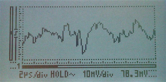
    Signal at the output (R14 = 110k, other resistors open) (some strong high frequency occurs)

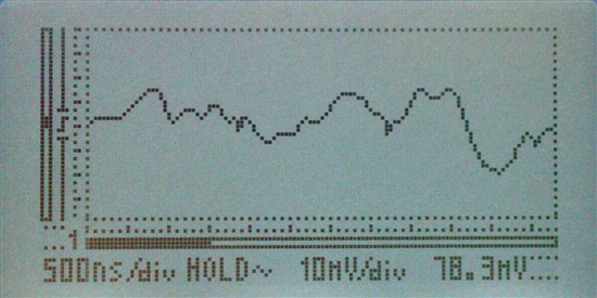
    Signal at the output (R14 = 110k, other resistors open) (timebase zoomed in)

    Measurement with external power supply (3.3V)

    Signal at the output (R14 = 110Ohm, R27 active)

    Measurement with power supply with 3V Lithium Battery

    Signal at the supply of the amp

    Signal at the reference

    Signal at the output (R14 = 0Ohm, all other resistors open)

    Signal at the output (R14 = 1100Ohm, R27 active)

    My interpretation

    The power supply seems to have a certain impact, as with the battery supply the noise goes down by 50%. Having R14 at around 100k and having the connection from RG to REFERENCE open seems to be wrong as high frequency noise is coming.

    Do you have any suggestions where to start?

  • Hello Christian,

    Let me summarize your application:

    Input: +/-4.6V
    Output: 0-2.38V centered about 1.19V
    Supply voltage: 5V

    In general I understand how you designed the circuit. First you divided down the input using the resistor dividers and then used an instrumentation amplifier to apply gain and bias the output.  You also had to reference the input to get into the common-mode range of the device.

    One of the attributes of an instrumentation amplifier is that they have very high input impedance (as opposed to a difference amplifier). However, that attribute is nullified by the resistor dividers.  Also, you have to be careful of the input common-mode voltage and output swing when using an instrumentation amplifier.

    Therefore I recommend evaluating the INA146. It is a difference amplifier with a differential gain of 0.1V/V (and the input impedance is 5 times greater than the original circuit).  

    Unlike most difference amplifiers, however, you can adjust the gain of the output amplifier, A2. With a single 5V supply, the common-mode input range is -25V to 19V, so there should be no issues there. My only concerns are that it has 3mV offset voltage (typical) and the output can swing to within 150mV of ground. However, you can adjust the gain accordingly so that 150mV represents an input of -4.6V.

    Please see attached TINA simulation. TINA-TI can be downloaded from www.ti.com/tina-ti.

    In the end I think the attached solution is simpler, uses integrated resistors to divide down the input signal, has higher input impedance, requires a simpler reference voltage circuit, and has a wide input common-mode range independent of the supply voltage.  You can still adjust the gain if desired.

    christian.TSC
  • Hi Pete,


    thanks for your suggestion.

    Regarding the input impedance, I think I forgot one detail (sorry for that): The connectors P1 and P2 with the 4.6V have 2.8MegaOhm resistors in series each to the connectors to the outside world. So the overal input impedance is about 5.6 MegaOhm. Input Voltages from the outside Volt are about 650Volts down to 0.1V (this is where the noise is becoming a serious problem)

    Regarding the INA146, it looks interesting, but we have a problem as the INA146 is double the price of the INA331. The unit is going into mass production and has two amplifiers, so this is a cost problem for us.

    Do you see any alternatives?

  • Hello Christian,

    Thanks for the clarification.  By placing the resistive voltage dividers on the input of the INA331 you have effectively changed the input impedance of the amplifier anyways.

    Nonetheless, your output will have artifacts of the waveforms that are present at your supply and reference pins.  The waveform at your reference pin will add directly to the output.  The waveform at the supply pin will be attenuated, or rejected, by the PSRR of the device.  Unfortunately it appears as though the frequency of the waveform present at the supply pin is ~200kHz.  There is little or no rejection at that frequency.  Please see the graph in the INA331 data sheet entitled "Power-Supply Rejection Ratio vs. Frequency".

     My suggestions are as follows: 

    1) Ensure you have proper power supply decoupling of the INA.  In other words, make sure you have a 0.1uF cap placed as close to the device's power supply pin as possible.

    2) You may want to add common-mode and differential-mode filters on the input after the signal is divided down. 

    3) Moving forward I suggest only evaluating the amplifier when it is in a recommended configuration.  In other words, ensure that R14 and R15 are both populated unless operating in a gain of 5V/V.  In that case, make sure R15 is not populated and R14 is shorted with a 0ohm resistor.

    4) You may want to look at the signals using a higher resolution o-scope to ensure you’re seeing the entire picture.


    I hope this helps.

  • Hi Pete,

    okay, we will go forward and try to improve the INA331's decoupling and also correct the usage of the amplification-setting resistors.

    At the moment, we have a 0,1uF cap at the GND (V-) pin of the INA331 between the GND-Plane and the VDD-Plane.

    If I understand the datasheet correctly, the cap has to be at the V+ Pin of the INA331? So we put it on the wrong side I assume.

    What do you recommend? Should the cap be directly at Pin 7 & 8? Should we leave, just to be shure, the other cap at the GND-Pin?

    Also I assume, each INA331 should have it's own set of caps?

  • Hello Christian,

    Thanks for the PCB layout. 

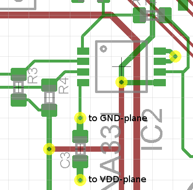
    No need for C3. Connect pin 4 directly to the GND plane. Place a capacitor as close to pins 7 and 8 as possible (right between the pins and the via). In general I prefer to see the supply voltage traces on the top layer with a ground-plane poured everywhere else on the top layer.

    For example, please see the picture below. It is from one of our TI Designs - Precision (TIPD101).


    Notice the placement of C3 and C4 with respect to pin 7 of U1. Those are the power supply decoupling caps. Also notice the power trace connecting to the capacitors before connecting to the pin. Finally, notice that a ground plane is poured on the top layer and stitching vias are added between the top layer and the ground plane (notice the GND vias right above C3/4 and right below pin 4 of U1.). Your ability to do this depends on the complexity of your design, of course.

    Yes, each IC on the board should have its own power supply decoupling caps.

    I hope this helps!

  • Hi Pete,

    thanks for your detailed answers so far. We will redesign our circuit and hopefully will have better results.

    Best regards,

    Christian