This thread has been locked.

If you have a related question, please click the "Ask a related question" button in the top right corner. The newly created question will be automatically linked to this question.

INA126 PA Strain Gauge Circuit

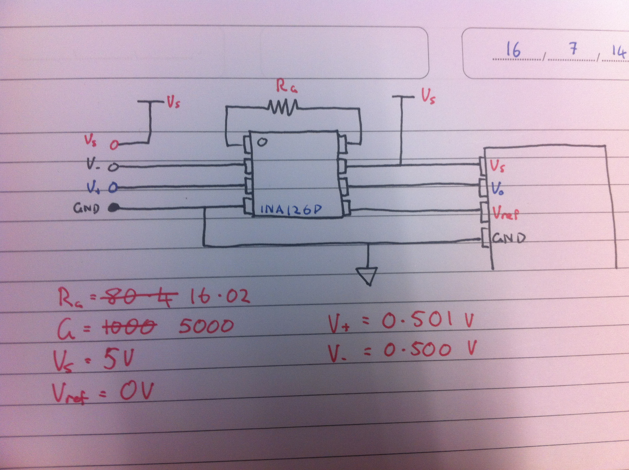
Hi, I'm trying to build a strain gauge circuit using an instrumental amplification IC (INA126PA), however the voltage outputs seem incorrect. Given voltage inputs of V+ = 0.501 mV,  V- = 0.500mV  and a gain of 5000 (Gain resistor = 18 ohms) I would expect to see about 5V at the output of the chip. Instead I get a value of 0.5V.

Varying the gain resistance or even removing the resistor altogether only has a very small effect on the output (Vo increases by about 20mV), which is what has me really confused.

I've included a circuit diagram below. The circuit is currently built on a breadboard. The input voltages are supplied by a USB NI-6009 DAQ and the input is recorded by this too. I have tried different positions on the board in case of poor connections and I have tried buying another chip in case it was faulty.

I feel like I must be missing something obvious. Can anyone identify a problem?

Regards,

Tim

  • Hi Tim,

    The problem is that the device is in violation of the Input Common Mode Voltage vs. Output Voltage. Please see the figure below.

    Having the device supplied with +5V and Ground, you will need to follow the limitations associated with the dashed line. This figure shows that for Vs=+5V/0V and Vref=2.5V the minimum common mode voltage is 1V (the device currently has a common mode voltage of 0.5V), but with that common mode voltage you will only be able to get an output of approximately 0.6V. To get the maximum output swing of approximately +0.6 to +4.3V the device must have a common mode voltage of approximately 1.5V.

    Here is what I recommend:

    Since you need a 1mV differential signal, apply 2.501V to IN+ and 2.500V to IN-. This will give the 1mV differential and it will also give a common mode voltage of approximately 2.5V ((2.501+2.500)/2). With a common mode voltage of 2.5V, the device is about right in the middle of the requirement for common mode voltage. This will give you a full swing of the output (~0.6V to ~4.3V).

    -Tim Claycomb

  • Thanks a lot Tim, that worked a treat!

    One further question: If I wanted to minimise the zero load output voltage, would I be best to increase the reference voltage to get that, or is there a better way to do it?

    (To clarify, I would like Vout to be as low as possible when V+ = V-.

  • Yes, you are correct and the reference voltage will need to be greater than 0.6V (the minimum output of the device).

    Since Vout=((V+)-(V-))*Gain+Vref and having Vref=0V, the equation simplifies to Vout=((V+)-(V-))*Gain. So when ((V+)-(V-))*Gain is less than 0.6V, the output will still be 0.6V (due to the limitations of the device). Adding a reference voltage will make the zero load point equal to the reference.  For example, if you have a differential voltage of 0V (no load) and a reference of 1V, the output will be 1V. Any differential voltage created (a load is added) will then be multiplied by the gain and added to the reference.

    Another way, although not always possible or desired, is to add a negative supply to the device. This way the output can swing both positive and negative and in your case you can have an output of 0V and you would not need a reference voltage.

    -Tim Claycomb

  • That answers my question perfectly Tim, thanks again.

    Regards,

    Tim J