This thread has been locked.

If you have a related question, please click the "Ask a related question" button in the top right corner. The newly created question will be automatically linked to this question.

high gain photodiode simulation --OPA365 spice model issue or real world issue?

Other Parts Discussed in Thread: OPA365
Hello, 

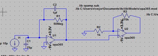
I am simulating a photodiode amp with 50Meg feedback resistor.  Photodiode modeled as 10pA
current source in parallel with 75pf cap to GND.  Current source in parallel with
cap are connected between inverting terminal of op-amp and gnd. 
Non-inverting terminal connected to ground.  Supplies set to +3 and -1V. 
Get larger error (from ideal) than when supplies are +/-2.5V.

Is this an OP365  model issue, or is this a real world phenomenon?.

  If so, what is it due to? The signals I'm dealing with are well within the

linear range of the op-amp (or so I think, ;-))


Thanks for the help.

Jorge

  • Hello Jorge,

    I did some simulation testing of the OPA365 transimpedance input stage in your circuit. When you change the supplies from the symmetrical +/-2.5 V condition, to the non-symmetrical +3.3 V/-1 V condition, you not only lower the voltage across the OPA365, but you also change the input common-mode voltage (CMV) point.

    The CMV is mid-scale, or 0 V, with the +/-2.5 V supplies. If the negative supply is referenced, the CMV is +2.5 V above its level. When the supplies are changed to +3.3 V/-1 V, the CMV is essentially shifted downward by -1.5 V because the OPA365 non-inverting input is still referenced to ground.

    Practical operational amplifiers do exhibit a shift in their voltage offset (Vos) as the CMV is moved across the amplifier's input CMV range. This results from the amplifier's non-ideal common-mode voltage rejection. Also, the input bias current may change with CMV. The 10 pA current that you have assigned is very low and is in a range comparable to the input bias current of the OPA365. These attributes will affect the voltage level observed at the amplifier output.

    My simulations show that the offset shift seen at the output of the OPA365 model due to a +/- 1.5 V CMV change, is about 250 uV. That error in conjunction of the real effects of Vos and Ib in the model results in the apparent gain error that you are observing. You can see the simulation results that I obtained in the attached image.

    The OPA365 model is complex, but probably isn't exact when it comes to exhibiting this behavior. But in reality real devices will exhibit behaviors of this nature. If you increase your photodiode current to higher levels the error will become less relavent.

    Regards, Thomas

    PA - Linear Applications Engineering