This thread has been locked.

If you have a related question, please click the "Ask a related question" button in the top right corner. The newly created question will be automatically linked to this question.

INA128 output load related distortion

Other Parts Discussed in Thread: INA128, LMV641

Re:  INA128 Load-related Distortion

I'm working on a board with a(n) INA128, I assume of Burr-Brown origin.

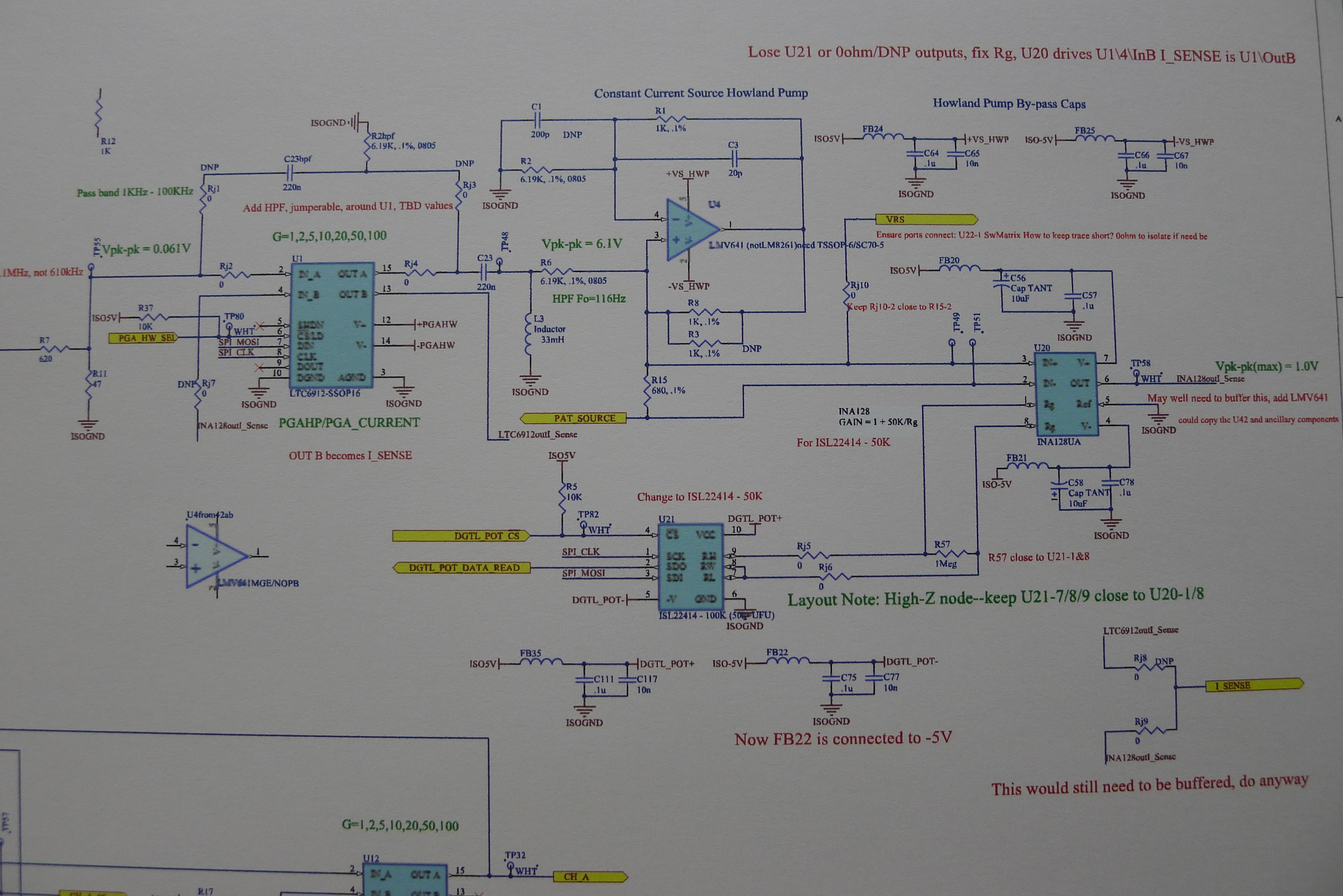
The device measures a voltage across a 680ohm resistor R15--see attached schematic photo, (1) L1010444INA128schematic.JPG--which is connected to GND via a(n) ADG636 switch, so there's another 155ohms to GND on the "bottom" of R15.  The purpose is to measure the sinusoidal current sourced from the Howland Pump.  The circuit uses multiple frequency sinusoids.  A microcontroller tunes the gain of the IN128 by means of a(n) ISL22414-100k digital pot.  (The -5V supply error to the pot has long since been corrected and the device replaced.)  The INA128 drives two capacitively-coupled multipliers, AD835, 1uF in series with 1k to GND at the X1 inputs of the multipliers.

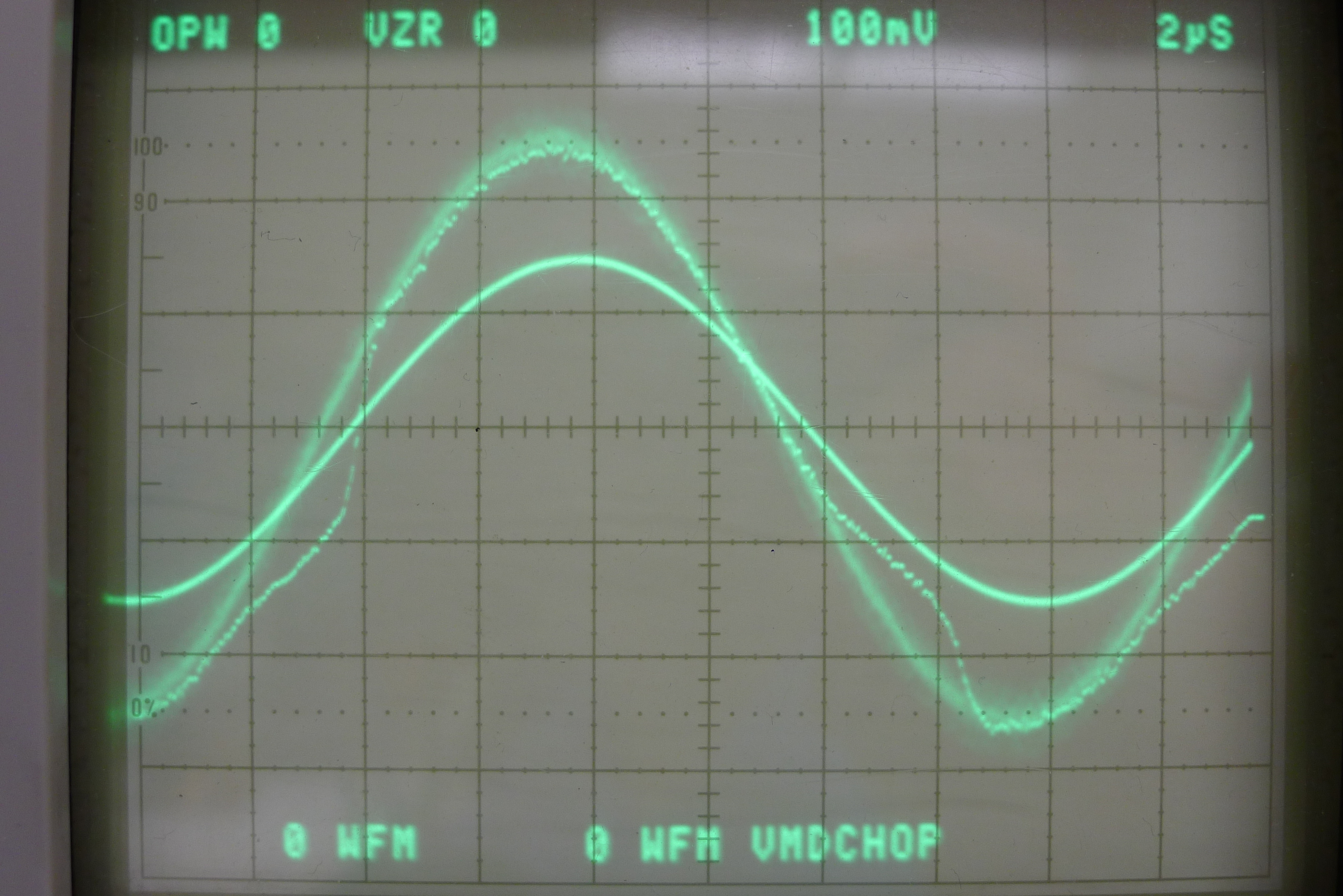
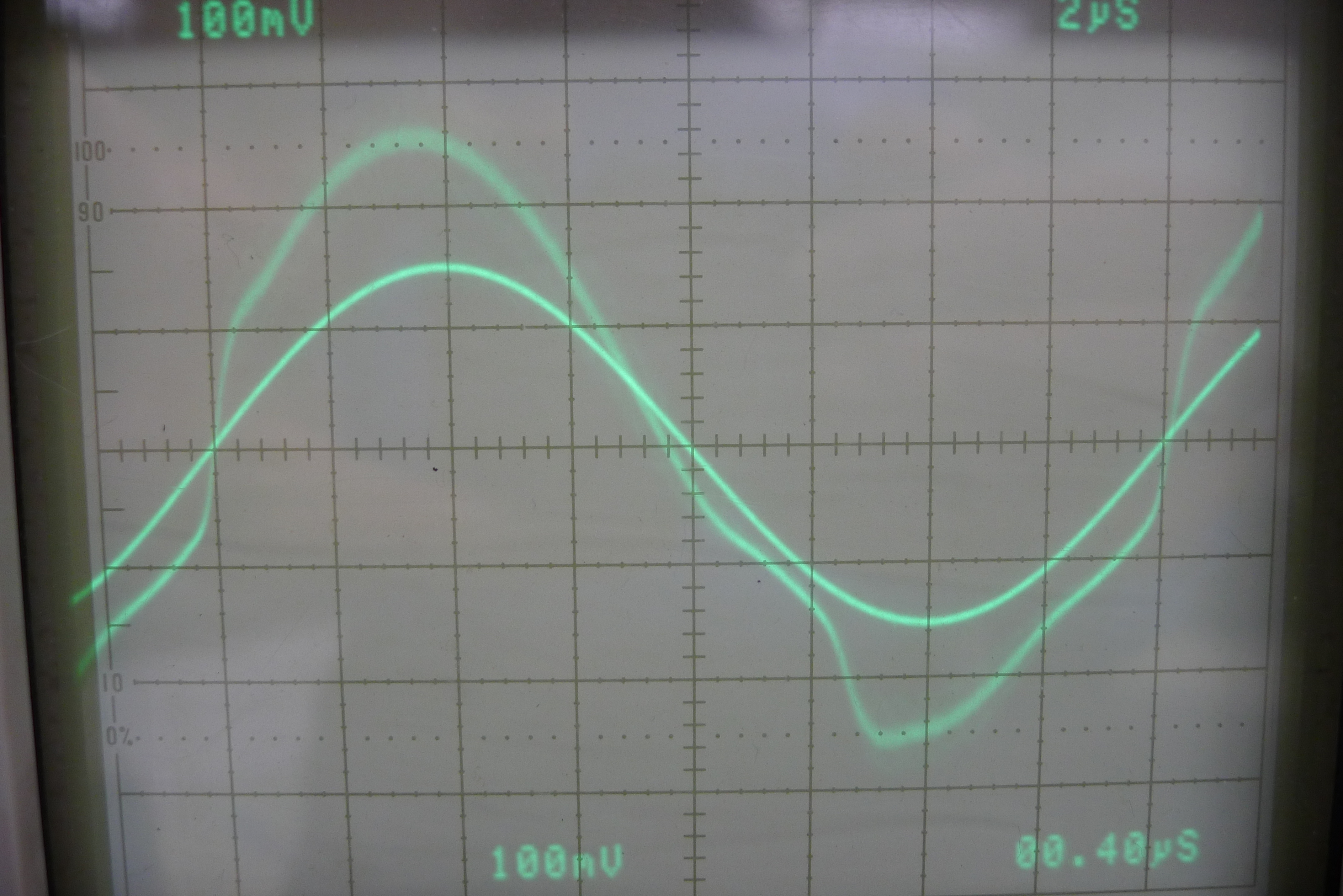
At low frequency, the INA128 output is a reasonable facsimile of the input, as can be seen in the attached photo (GND is the center line of all 'scope photos), (#1) L101441_2kHz.JPG, showing a 2kHz sinusoid, the "inner," undistorted sine is the INA128 input (measured differentially across R15 with a 7A13 differential comparator plug-in in a TEK 7854 mainframe), the "outer" is the output (single-ended via 7A26).  Careful inspection of (#2) L101439_2kHz.JPG reveals a small "kink" in the positive slope, negative voltage in the first grid southwest of the intersection of the center graticule lines.

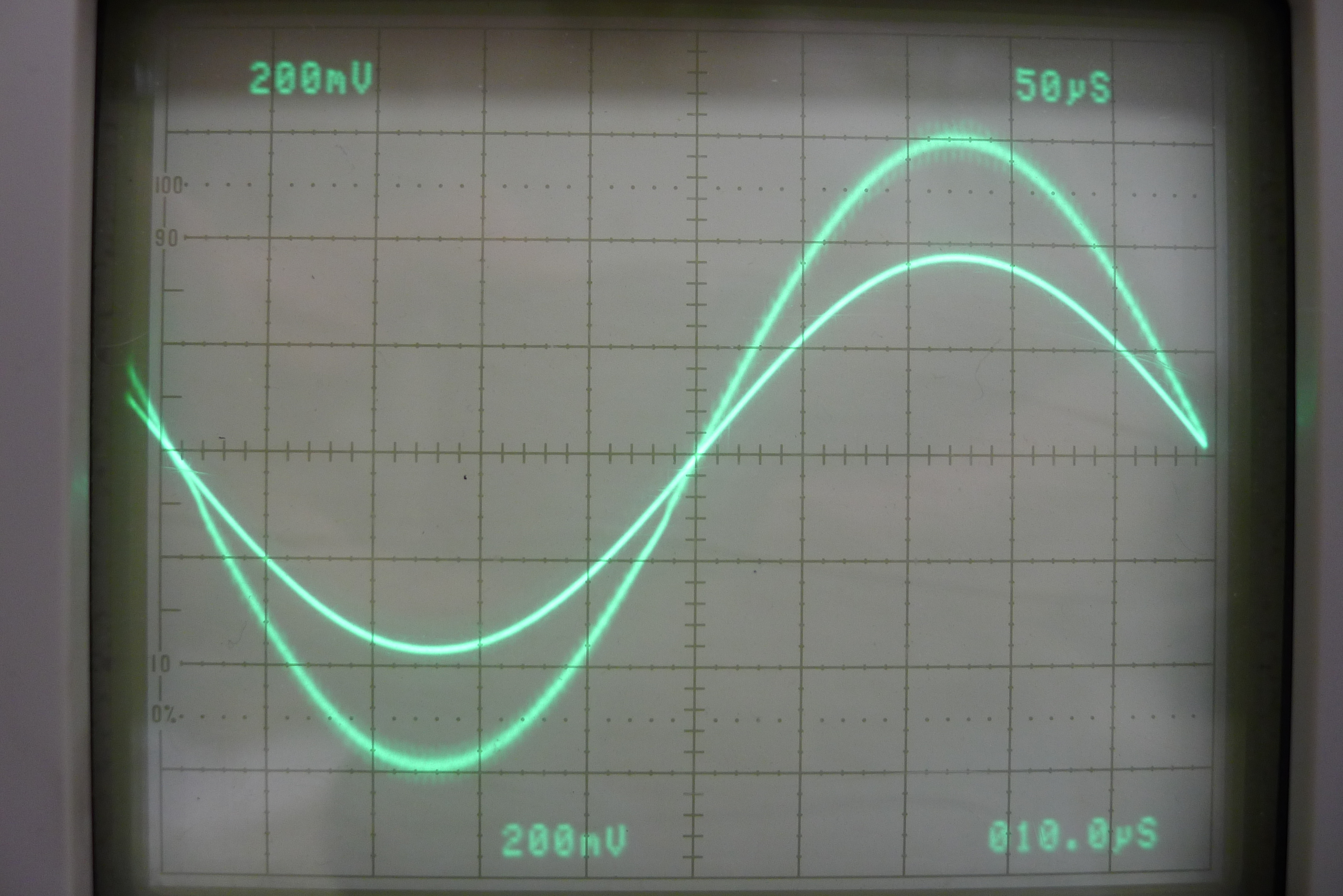
At higher frequencies, 62kHz shown, there is considerable distortion especially of the negative portion of the sinusoid, as seen in (#4) L101443_62kHz.JPG.

I've considered slewing, load, power supply, and done several experiments.  Changing the gain reveals the same effect, as does changing the load with resistors directly connected from the INA128 output pin to GND.  I've also added resistors to the inputs on the hypothesis that input biasing could be the cause.  None of these tests changed the shape of the negative sinusoidal output of the INA128.

Upon disconnecting the multiplier loads, by lifting the INA128 output pin (U20.6), from the board the output now looks like a reasonable sinusoid.  A 'scope photo, (#5 L1010447_OC.JPG shows the undistorted open-circuit U20.6 output with the distorted, loaded U20.6 output at 62kHz.  Loading U20.6 with 1kohm is no different--nice output.

Clearly, the INA128 is not pleased with the load applied.  Do I need to buffer the output?  What is wrong with the load and how best to attain a distortion-free output?

(1) L1010444INA128schematic.JPG

(2) L1010441_2kHz.JPG

(3) L101439_2kHz.JPG

(4) L101443_62kHz.JPG

(5) L1010447_OC.JPG

  • Hello Arne,

    Thanks for all the detailed information and scope shots.

    This looks to me like slew-induced distortion since it appears to be gain and frequency dependent. Please refer to the "Maximum output voltage vs. Frequency" graph in the INA128 data sheet. Please note that your supply voltages are different than those used in the data sheet. In addition, notice how the curves vary for different gains. This is important because it appears as though your design uses multiple gains. Finally, note that the graph is generated with a load resistor of 10kohms. It appears as though you have a complex load impedance, therefore performance in the "Maximum output voltage vs. Frequency" graph is not assured. Therefore, I recommend running some additional experiments similar to #5 (disconnected load). However, I would try using a load resistor of 10kohms and varying the gain and frequency to see at what point(s) the output distorts. If you cannot get the output to distort, then I do suspect the complex output impedance is having an affect on the INA128 output stage's ability to slew given the different gain and input frequencies. Buffering the output (as you suggested) will provide the INA128 with a high impedance node to drive, which should fix the issue. However, you must ensure that the amplifier you select to drive the AD835 has sufficient full power bandwidth. You also may have to consider lowering the gain of the INA and applying gain with the output amplifier (no longer would it be called a buffer). It really depends on the gains, frequencies, and peak amplitude of the output. Please see the attached slides for some additional information.

    I hope this helps!

    Slew induced distortion.pptx
  • Pete,

    Thanks for the reply.  I'd considered slew-rate-induced distortion, and remedies, as in buffering the output.  The circuit changes the frequency and the gain in unison, so further experiments are a little cumbersome, but doable.  I’ll have another look. 

    Given the poor tempco of the ISL22414, not to mention the sensitivity of the high-Z INA128 inputs, I'm planning to redo the circuit like this:

    Fix Rg (INA128-pins 1&8), lose the digital pot (turns out that much gain adjustment is unnecessary), and keep that node tight.

    From the attached schematic photo you can see there’s a PGA, LTC6912 with one unused channel, IN/OUT_B.  The input impedance is 1kohm.  (After my open-circuit INA128 measurement, I added 1kohm to GND on the output, and the output was still not visibly distorted at the higher frequency, so I'm confident the LTC6912 load on the INA128 won't be a problem.)  I can drive the INA128 output into this channel for my variable gain, then drive the AD835s with the LTC6912.  Assuming, of course, that the LTC part doesn’t have a similar slewing problem.  P^)

    I can test this out without too much work on the present prototype, to see if I need to buffer the multiplier loads regardless.  I have available an LMV641 and can try this out for driving the multipliers.

    Arne