This thread has been locked.

If you have a related question, please click the "Ask a related question" button in the top right corner. The newly created question will be automatically linked to this question.

Best transimpedance multiplexing technique with OPA842/OPA847 (highly dynamic TIA)

Other Parts Discussed in Thread: OPA846, OPA842, TINA-TI, OPA657, OPA656, OPA857, TS5A3357, OPA847, OPA861, LMH6504

Dear all,
I have troubles in managing a photodiode application with a very high dynamic input.
Here are my specifications :
Photodiode : Rsh=1G, capacitance=15pF (under 100V bias), darkcurrent=20nA.

Range of measurements : I'd like to measure pulses (more or less 20ns width) from just above dark current (100nA) to very high energy pulses (10mA). Bandwidth : more than 30MHz.

I also have a DC component going from 0mA to 10mA (I already did my best to optically remove as much as ambient light as possible).

The sampling is done using a ADC at 100MHz - 14bits.

I'd like to keep the shape of the pulse (no distorsion and linearity with pulse height), therefore a transimpedance with diodes in the feedback path are not possible.

The problems are the following : It's easy to make a transimpedance that works for high signals (using a OPA482 with a transimpedance of 300 Ohm and a DC servo to remove the DC component  and avoid saturating the op amp). I get a nice 80uV total noise. It's easy to make a transimpedance that works for small signals (using a OPA846 with a transimpedance of 10kOhm). I get a nice 600uV total noise.

 
I tried a lot of things : put some analog switches in the photodiode path (but C_sd is a real problem), put some analog switches in the feedback path (but again c_sd is a problem due to my bandwidth requirements), use a tee network to be able to dynamically change the transimpedance (but it destroys my bandwidth). I'd like to avoid any mechanical relay.

The only possibility that I see is to always use the transimpedance of 300Ohm and add gains afterwards. With a small signal of 100nA this gives 100nA*200Ohm=20uV which is inside the 80uV OPA842 total noise. This solution works but it does not meet my specifications.

Attached file is a Tina-Ti file with both implementations (OPA842-OPA847) with both DC servos and VMUX setting/Parameter stepping to show two curves on AC analysis and noise analysis.


Any thoughts?

Best regards,

MJMJ1.TSC

  • Hello Matthew,

     Interesting problem. Can you please show me how you used the switches in the feedback path? If you insert the switch between the inverting terminal of the opamp and the feedback resistor then the voltage across the switch should stay fairly constant, which should minimize the effect of capacitance.

    Rather than using 2 different amplifiers can you not use just one amp. with one switch and compensate it accordingly based on the feedback resistance chosen? The switch would be on the 300Ohm leg.

    Have you looked into the OPA656/OPA657? These are JFET amplifiers and should minimize any offsets due to the amplifiers bias current.

    -Samir

  • MJ2.TSCHello,

    Yes at first I thought about using only one opamp. I tried the following with analog switches:

    - Put one between the inverting input in the resistor 10K  (like inside the OPA857)

    - Put one alternate switch between the two legs to the opamp-output

    - Put two alternate switches between the two legs to the opamp-output (like explained by Luis Orozco of Analog Devices in www.analog.com/library/analogdialogue/archives/47-05/pgtia.html )

    - Put one alternate switch to select two different opamps (like on the attached file in the first post but with analog switches).

    The problem is not the variation of voltage at the contacts of the analog switch but the C_sd inside the analog switch. I have attached a trial with TS5A3357 (single supply but I connected it between +2.5 and -2.5).You can see in the AC analysis of the new attached file that at low gain (switch is on) this works OK. But at high gain (switch open), it reachs well +80dB (10K TIA) but falls just afterwards because C_sd start to conduct and the TIA starts to decrease (that is why off-isolation is not good in analog switches at high frequency). Look at the Tina attached file.

    About OPA657: I agree that this 1.6GHz JFET amplifier will have no bias current and therefore no input noise spectral density. However performances seems to be better with OPA846/OPA847 (see TI's Application Note SBOA122 of Xavier Ramus).

    This is also confirmed with the online spreadsheet : www.jensign.com/noise/cumulative.html

    Chosen parameters for OPA847 : Input voltage noise spectral density : 0.85nV/sqrtHz, Input current noise spectral density : 2.5 pA/sqrtHz, GPW : 3900MHz, Rf=10k,Ci=15pF,Cp=0.6pF I get a total noise of 338uV (f3dB=30MHz).

    Chosen parameters for OPA657 : Input voltage noise spectral density : 4.8nV/sqrtHz, Input current noise spectral density : 0.001 pA/sqrtHz, GPW : 1600MHz, Rf=10k,Ci=15pF,Cp=0.7pF I get a total noise of 1136uV (f3dB=30MHz).

    However I think that I might live with noise of the OP657 if the "no bias" really improves in one way the mitigation of the high dynamic.

    I have a new idea : Would it be possible to keep always the high transimpedance (10K) and attenuate the input current when I have too much signal? Using a resistor and a OPA861 (transconductance amplifier to regenerate a current) and then a transimpedance (OPA847) seems to give good results at first. But i have no experience with transconductance amplifiers.

    Best regards,

    MJ

  • Hi Matthew,
    I am not sure I understand the transconductance amp. scenario. Can you please draw it out? Another thought I had was, can we use an amplifier with a Power Down/Disable pin. This usually puts the amplifier in high output impedance state. It is generally not recommended to use
    the Power Down pin as a multiplexer, but if you can make it work in the application..why not.
    -Samir
  • Hello Samir,
    Something like :
    Bias(150V)->Photodiode (Cd=15pF) -> Resistance of 50Ohm between photodiode_anode and GND. A OPA861 connected to the photodiode_anode and a R1/R2 on the OPA861 to be able to lower the current. R1/R2 is configurable.
    The output of the transconductance OPA861 is a current then goes to a fixed transimpedance OPA847 10k stage.

    Otherwise I also looked at CLC5543 (replaced now with http://www.ti.com.cn/cn/lit/ds/symlink/lmh6504.pdf ). It might be another possiblity, but its high dependance on temperature might be a problem.

    Yes, we can use OP with powerdown/disable. I thought also about that and OPA847 has one. However It's explicitly discouraged in the datasheet to use the powerdown/disable pin as a multiplexer. OPA842 doesn't have powerdown/disable pin but i'm sure that it's possible to find an equivalent.
  • Hello,

    I'm back to this topic, however i still don"t have any idea how to manage these requirements?

    Has anyone have a good idea?

    Thanks


    Best regards,

    MJ

  • Hi Matthew,

    Couple of ideas:

    1. Post Amplifier with variable gain:

    I found this older E2E post which has some suggestion on a post amplifier with adjustable gain settings, I thought I share with you:

    http://e2e.ti.com/support/amplifiers/high_speed_amplifiers/f/10/t/305109

    TINA-TI file in that post:

    http://e2e.ti.com/cfs-file.ashx/__key/communityserver-discussions-components-files/10/2664.OPA695-VGA-attenuator-6_2D00_8_2D00_2011.TSC

    2. Varying the Gain using Single TIA stage with Analog Switch:

    Also, I'm thinking you might be able to select your TIA gain, by doing the following:

    a) Isolating the Photodiode + switch capacitance from TIA input using a BJT in Common Base mode

    b) Switching in additional CB stages, as needed, to divert a percentage of the PD current for conditions where your signal amplitude is large

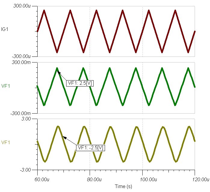
    I've shown this below with some notes within the schematic:

    Resulting output for the two switch positions:

    Here is the TINA-TI file for the circuit above:

    /cfs-file/__key/communityserver-discussions-components-files/14/7870.TIA-with-Variable-Gain-Hooman-2_5F00_23_5F00_15.TSC

    I hope this is helpful.

    Regards,

    Hooman