This thread has been locked.

If you have a related question, please click the "Ask a related question" button in the top right corner. The newly created question will be automatically linked to this question.

This question involves the possibility of the transistors in a LMV774 Op-Amp latching in the event of an EOS, ESD, Transient, etc...

Other Parts Discussed in Thread: LMV774

To whomever reviews this post,

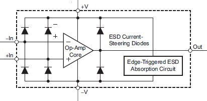
I had a question in regards to TI's LMV774 series op-amp. I cannot provide schematics, subsystems, etc because all of this information is disclosed.

I am trying to diagnose why an intermittent failure occurred in a 4-20mA transmitter. The output of the failed unit was pinned at a very low mA output. At the time of the failure, severe thunderstorms were present in the area. The unit was unplugged and then powered back on and the unit did not recover to it's normal operation. After opening up the device (a welded housing), I noticed the LMV774 Op-Amp on the PCB had a scorch mark on it's surface. This brown discoloration indicates that this part was overheated. Given the nature of the weather, I suppose the unit saw an ESD, Surge, etc. Since the unit operates through a current loop, it is not grounded. When I probed the LMV774 op-amp, I noticed the pin out voltages were correct. 

**Is it possible for an LMV774 op-amp's CMOS transistors to latch-up in the event of a transient or surge and not be damaged? Note: As soon as I probed the OP-AMP and discovered it was still functioning, I checked the overall output of the unit and it began functioning again. The output was no longer pinned and the unit resumed normal operation. Since the device is not grounded, perhaps by touching the PCB I grounded the Op-Amp's terminals and this dissipated the potential energy stored in the latched transistors?


I am trying to provide an explanation as to what caused the unit to fail. Since the failure was intermittent and not permanent, it is really hard to provide an explanation. Since the output was pinned at a specific output independent of the devices input, it leads me to believe that the OP-AMP was indeed latched.

My main question is whether these theories regarding why the unit failed are plausible. Essentially, is it possible for the LMV774 to latch up during the event of a transient or surge? If it can latch, does this mean that all of the pins are shorted to the negative terminal of the unit since no bias is applied to the transistors to change their state? When latched, can the Op-Amp self recover or does the unit need to be grounded to PE? Does this brown scorch mark indicate overheating do to a transient event or could this simply be from heat wave soldering?


It is very important whether this scenario is plausible so that a proper Engineering Report regarding this failure can be written for my customer. Although I cannot disclose information publicly, I would be more than willing to answer questions over the phone. I would actually prefer to discuss this issue over the phone with an engineer representing TI. The customer support can only answer questions regarding the datasheet. I was told the only way I can contact an engineer was through the E2E forum. Again this matter is urgent and any help or opinions would be greatly appreciated.

Keith Oldano

(Electrical Engineering)

973-616-6938

  • Hi Keith,

    Below is the typical ESD protection on modern devices.


    The "diodes" are ESD structures from each input or output pin to each supply. These clamp any excess voltage (>0.5V) to the respective supply line.

    Across the supply line is a larger protection structure. If the voltage between the V- and V+ lines rises quickly (<1V/us), it clamps the supplies together.

    Keep in mind the ESD strictures are there to protect the op-amp - not the circuit. The structures work together to keep the voltage across the die to a safe level for the circuits on the die.

    It is possible for ANY integrated circuit to latch-up if the external transients overwhelm the protection (as in a "Natural ESD event from the sky" ). Latching-up is not necessarily destructive, but it is damaging, particularly if it causes excess currents to flow through places that were not designed to handle (any) currents..

    The device may seem to still be "functioning", but you may find it has been "impaired" at some point (high offset voltage, reduced output drive, instability, high bias currents, etc). Most likely it will no longer meet datasheet specs.

    If enough supply/source current is available, it is possible for the device to heat up short of melting and still operate ("Operate" means it still wiggles - but not as well as before). Silicon can survive well past 150°C, though usually not the packages or PCB. I have seen devices heat up and "burn" the board below, and still "work" afterwards.

    The latch-up occurs as long as current is still applied after the event. Removing power "resets" the latch to "normal" operation. Assuming you had to cut the welded case apart - the time was probably longer than a few minutes. I doubt if it "stored" charge internally for that long - but I would not rule it out.

    What was the condition of the other three amps (LMV774 is a quad)? The four amps share a common bias circuit - so if one of the other channels is having "issues", it could be causing problems with the internal biasing for the other amps. What were the other three amps doing at the time it "recovered"?

    Does it look like the "flash" is from one point to another?

    Does the LMV774 get warm now? Does the circuit draw more supply current?

    Is the soldering on the leads still shiny (look like like the non-damaged devices). The leads on device that overheats for a while tend to loose their "luster".

    Can you provide a photo of the "mark"? Do other non-zapped boards have the same mark? If it is a wave soldering issue, other boards may show the same mark.

    Do any of the "protection" equipment (diodes, gas tubes, transorbs, air-gaps, etc...assuming the have them) show signs of stress?

    Without knowing the exact failure mode, the FA/Process folks are going to be reluctant to issue any opinions.

    Regards,

  • Paul,


    Thank you for responding so quickly, I really appreciate all of your feedback as it has been more than helpful. Above is a picture of the "scorch" mark on the Op-Amp. Our circuitry has a voltage regulator, transient voltage suppressor, as well as reverse polarity protection. I believe the TVS clamps at 48 Vdc and begins to breakdown at 33 Vdc min. The voltage regulator did not appear damaged and output a normal operating voltage of around 4.97Vdc (the input to the device is 9-30 VDC and the voltage regulator steps this down to 5Vdc.) If you look at the discoloration on the Op-Amp, you will see that it appears to be located in the center. After a quick check, no other PCB's in stock have this discoloration so that eliminates the heat wave soldering theory. The TVS and reverse polarity protecting diodes should have shunted any surges or transients from the internals of the device. If the pulse was rather quick then perhaps the rest of the circuit could have seen the surge however this would have most likely destroyed the voltage regulator. I believe? With protection of the overall circuit and protection on the Op-Amp itself, I am lead to believe that somehow the Op-Amp was overheated, perhaps over time (Note: this unit was running 24/7 for 6 months before failing; it just so happens that a sever lighting storm was present which makes all of these theories iffy). The other possibility is that an ESD occurred to the outside of the device (not through the terminals of the connector) and arched through the housing and to the PCB. This would negate any overvoltage, reverse polarity, etc. protection. 


    Again, I can't stress enough how much I appreciate your assistance in diagnosing the root of this intermittent failure. Tomorrow I will check to see if the op-amp is impaired in anyway, as well as check for any pins that lack any luster. I will also see if any drift occurs when the input remains static. Have a great rest of your night.

    -Keith

  • Hi Keith,

    The picture did not make it through (you must have 'pasted" it in). You have to click the "Use Rich Formatting" link in the lower right below and click the "Insert/Edit media" icon to the left of the paperclip icon to insert a picture file (TIF/GIP/JPG/PNG). Not convenient..I know..but that is what we are stuck with...

    Is the opamp driving the 4-20mA, or receiving? If driving, I assume there is an external pass transistor?

    A quick check of the op-amp is to check it's offset votlage, A quick way is to place it in a "normal" operating condition (not railed or some non-linear mode) and use a good millivolt meter to measure offset voltage directly across the input pins (+IN and -IN). At room temp, if it is greater than ±1mV, then it is bad. Any damage to the input stage generally causes an increase in offset voltage.

    Regards,

  • Paul,

    Sorry for the delay in terms of the picture. I figured the picture would be fine to be pasted in a HTML "Word Environment". Attached is the picture of the scorched Op-Amp. Like I said yesterday, it starts from the center and spreads outward and decreases in intensity. It does not look like a "flash".

    Sometime this morning I will be meeting with other engineers at my company to discuss some of the information that you provided. If we have any questions during our meeting, would it be possible to give you a call. I feel this would be a more effective means of communicating and diagnosing the root of this intermittent failure. I will have to talk to the VP of engineering but I might also be able to provide you with the schematic to our transmitter.

    Thanks again,

    Keith Oldano

    Electrical Engineering

    Sigma-Netics Inc.

    Two North Corporate Drive

    Riverdale, NJ 07457

    973-616-6938

    koldano@sigmanetics.com