This thread has been locked.

If you have a related question, please click the "Ask a related question" button in the top right corner. The newly created question will be automatically linked to this question.

OPA454 - Cannot enable output; E/D draws large current

Other Parts Discussed in Thread: LM2904, OPA454

Hello TI Community,

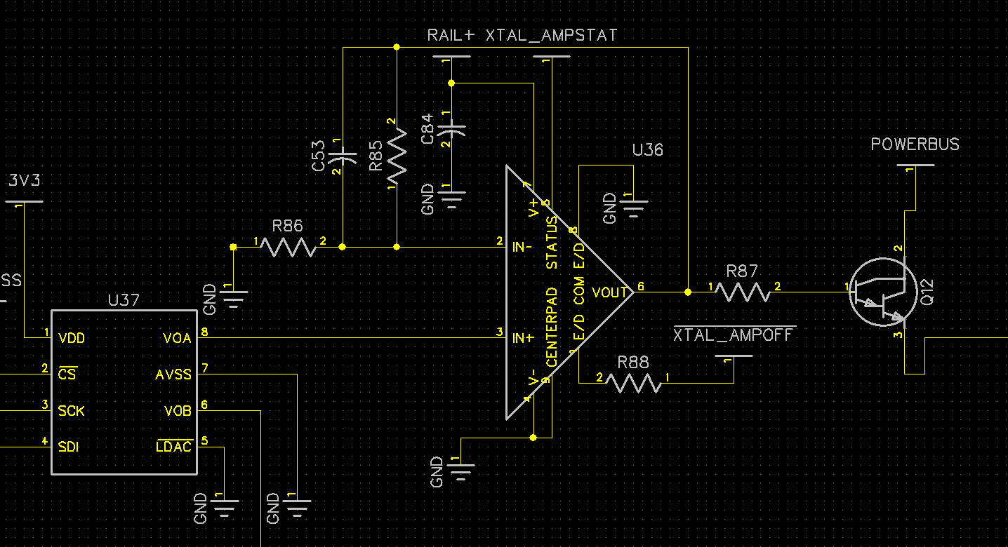
I have a slowly varying DC signal (from a DAC) that I need to amplify and pass to a voltage follower to provide a 0-42V, 0-3A output. I simulated the design using National Instruments MultiSim and tested with an LM2904 amp (only to 20V). I then laid out my PCB and built it up, using 4 OPA454s for (4) 0-42V outputs.

Unfortunately, none of them work. The signal from the DAC is present. The voltage rails on the OPA454 are +48V and 0V. However, I am unable to enable the output. The E/D Com pin is connected to ground but the E/D pin floats at about 0.35V without being driven. If I try driving it with 5V, I can only develop about 0.9V (driven from a 5V 50 ohm signal). The output is sourcing a significant amount of current. If I just measure the resistance between the E/D and E/D Com pins, I get about 450 ohms on the 4 placed ICs plus one IC that has not been previously handled. When I remove the ICs from the board, the pads measure >36 MOhms, so it doesn't seem to be a problem with the board.

What am I doing wrong?!

Schematic:

  • Well son of a gun... I just realized my mistake. I confused myself with the pattern in my component library. Pin 1 is the E/D common and should be connected to ground. Pin 8 is the E/D that should be connected to logic. I made up the pattern, verified it with the datasheet and then worked a couple of days on a different project. I came back and saw the "COM E/D" for pin 8 and thought that was the common. <sigh>
  • Hi Thomas,

    Glad you figured it out on your own. I hope the rest of it goes smoothly for you.

    Don't hesitate if you do need something from us.

    Regards, Thomas

    PA - Linear Applications Engineering

  • Hi Thomas,

    I am now experiencing a new issue with the OPA454. Could you please review the schematic above and see if anything jumps out at you? The values for associated components are below. Currently, the output from the amplifier remains low until the input reaches about 1.9V, at which point the output swings to the positive voltage rail. On my test bench, the positive voltage rail is 25V.

    R85 = 22k ohm

    R86 = 1k ohm

    C53 = 0.01 uF

    Edit to add: it seems to latch to the positive rail. My DAC is slowly changing the output voltage from 0 to 2.048V before wrapping around to 0 again. It hits the rail at about 1.9V and then remains at the rail when the DAC wraps around to 0. When the DAC climbs back to about 1.2V, the output swings to the negative rail (ground) and remains at ground until 1.9V where it swings to the positive rail, ad nauseum. 

    Thanks!

    ~Tom

  • I think I need to get more sleep or more coffee... I'd like to run this by the experts here but I think I found my second problem:

    I had a mistake in the PCB design files where the center pad was connected to ground instead of V- (which was supposed to be -5V from a small switched cap charge pump). Since those center pads are actually connected to V- internally, I was shorting out my charge pump. I removed the charge pump and jumped the "output" to ground, effectively changing the op-amp negative rail from -5V to 0V.

    Now I am trying to amplify a signal starting at 0V. But the allowed negative Vcm is V- + 2.5V, so the amp isn't in the linear region until the signal is approaching this value (~2V). However, I have a gain of 23 so it immediately rails.

    Sadly, there are thermal vias connecting the center pad to ground so it looks like I will have to respin the board.
  • Hi Thomas,

    I went through each of your corespondences and followed your progression. It appears that you have all of the pins correctly identified and how they need to be connected. Also, as you know, the OPA454 PowerPad must be connected the V- potential for proper operation.

    The OPA454 lower common-mode voltage limit will be an issue if your input voltage is ground referenced (0 V) and the V- pin is at 0 V too. Your idea to include the -5 V charge pump for the V- supply would solve that problem. The output would then follow the input with a gain of 23 V/V. It would increase until it rails with an input level approaching +2 V.

    If you do use the -5 V charge pump to provide V- make sure the E/S common is referenced to it, and the PowerPad is connected to it.

    Let me know how it all works out.

    Regards, Thomas

    PA - Linear Applications Engineering

  • Hi Thomas,

    As an interim solution (before ordering new PCBs), I cut some 0.001" copper foil to create a new land pattern for the parts. With a little super glue and some 36 awg wire, I was able to rework the board and get things working.

    Right now, I have E/D COM referenced to ground so I can use a logic level signal from a microcontroller to enable/disable the device. I tested it yesterday and it works great. I have a clean, stable linear (within the constraints of the DAC, anyway) output that varies from 0 to 46 volts.

    Thank you for your help along the way!

    ~Tom

  • Hi Thomas,

    Great - thanks for the feedback! it looks like you are well on you way with the OPA454. Hopefully, everything will go smoothly from here on out.

    Regards, Thomas

    PA - Linear Applications Engineering