This thread has been locked.

If you have a related question, please click the "Ask a related question" button in the top right corner. The newly created question will be automatically linked to this question.

Help please, ACF2101 not integrating

Other Parts Discussed in Thread: ACF2101, LM741

Hi there,


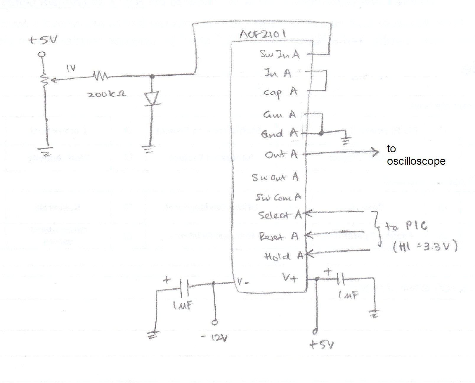
I am having some problems getting the  ACF2101 switched integrator to integrate. I've tried my best to troubleshoot but couldn't figure it out and am hoping that someone here can point out my mistake or give me some advice. I have it connected basically as in Figure 12 (Using the ACF2101 with a Voltage Source) in the datasheet, except that R1 is connected to 1V out from a potentiometer which is connected to +5V supply. Also, I have do not have capacitor C1, but I have a Schottky diode for D1 (1N5819, tested forward voltage drop of 0.02V)


http://focus.ti.com/docs/prod/folders/print/acf2101.html


I have the select, hold and reset pins controlled by a PIC microcontroller (outputs 3.3V), and it is powered by +-5V supply.This SOIC chip is soldered onto a SOIC to DIL adaptor and connected on a breadboard for testing.

When I put it in Integrate mode, I would expect that the voltage should integrate until it reaches the negative limit of -5V. However, on the oscilloscope I only get milivolts and this voltage does not seem to change when the IC is in any mode.

In INTEGRATE mode, a HI is sent to the reset switch and a LO is sent to the Reset switch but when I measure the voltage at the pins, both voltages are at 0.29V. However, when in HOLD mode, both switches are sent HI signals and the pins will be at 3.3V.


Any ideas would be greatly appreciated. Thanks.

  • Hello,

    I have reviewed your description of your AFC2101 circuit connection and in general it sounds like you have most everything covered. However, there is one thing that is not clear to me. You mention, "and it is powered by +-5V supply." Are you speaking of the PIC microcontroller, or the ACF2101 supply? If you are speaking of the ACF2101, then that is a problem. It requires a minimum of -10V on the -V pin to be properly biased for operation. If your -V supply is -10V to -18V, then there is another problem awaiting discovery.

    Regards,

    Thomas

    PA - Linear Applications Engineering 


  •  

    Thanks for the reply. Yes, currently I have it connected to +5V and -5V; I thought that would be sufficient as in my application I would only need it to integrate up to -3.3V. 

    Well, I guess I have misunderstood the datasheet (because I saw that it says +- 18V?). Great, if that's the case, then it should work when I change the supply voltages. What voltage levels do you recommend for the supply ?

    Thanks again, I will make the changes and see how it goes.


  •  

    Thomas,

    I've changed the -V supply to -13V and kept +V supply at 5V but unfortunately the result is still the same.Do I need any other components in the circuit ? I've also tried with an LM741 as an output buffer.

  • Hi,

    Okay, now that you have the negative supply at a usable voltage we can figure out what else is going on in the circuit. Let's assume for now that your timing set-up is correct - actually a timing diagram might help if you have one.

    Using the ACF2101 in the voltage-input mode brings certain limitations that the data-sheet discusses on page 13. You mentioned in your earlier discussion that you are using the Schottky diode at the input and you measured a forward voltage of 0.02V - which by the way seems very low. Also, you mentioned something about adjusting the voltage from the potentiometer to 1V. The data-sheet diagram (Fig. 12) shows the Schottky connected from the ACF2101 input to ground. So it is not clear what voltage level you are applying to the integrator input. The voltage-input mode discussion cautions about what happens when the input voltage exceeds 0.4V.

    It shouldn't be necessary to buffer the ACF2101 output unless you need a current or voltage level beyond the capabilities of the device.

    Thomas


  • Thomas,


    Please find attached a simple sketch of my connections. The resistor R1 is connected to +1V.

    Okay, now with a negative supply of -12V and with diode D1 removed, I see that the chip manages to integrate when in Hold mode (which is what is expected as in the datasheet). So I guess the problem here is that the diode is diverting the current to ground.

    I have a few questions and hopefully you can clear things up for me;

    1) I guess that I need both D1 and C1 here ? As the datasheet states the addition of "either C1 or D1" for proper operation. How do I go about determining/calculating the correct capacitance to use ? How is the current prevented from going straight through diode D1 to ground ?

    2) I've always thought that voltage-input mode would be the main method of using the ACF2101. How would the internal cap be charged with other inputs methods, other than with a voltage or current source ?

    3) If the input pin voltage can never exceed 0.4V, how does the example in the datasheet work ? Doesn't capacitor C1 charge up to near 10V ?

    In my application, with voltage source value constant, I need to be able to get  varying integration times when the resistance is varied.

    Thanks for your time,

    Melvin.

  • Any ideas, Thomas ?

    I really need your help as I cannot find any useful information anywhere.

    Thanks.

  • Hello Melvin,

    I apologize for not getting back to you sooner; I was out a couple of days. I am going to repeat your questions here so that I may address them one at a time.

    Okay, now with a negative supply of -12V and with diode D1 removed, I see that the chip manages to integrate when in Hold mode (which is what is expected as in the datasheet). So I guess the problem here is that the diode is diverting the current to ground.

    If the diode is removed and the input exceeds +0.5V the hold switch will conduct. The ACF2102 will integrate under that condition as explained in the data-sheet. When the Schottky diode is added into the circuit and the applied voltage is near zero the current will be primarily directed to the integrator input. But as the input source charges the diode capacitance and the voltages rises the diode will become more forward biased. Then current will begin to be diverted through the Schottky diode to ground.

    I have a few questions and hopefully you can clear things up for me;

    1) I guess that I need both D1 and C1 here ? As the datasheet states the addition of "either C1 or D1" for proper operation. How do I go about determining/calculating the correct capacitance to use ? How is the current prevented from going straight through diode D1 to ground ?

    The voltage implementation has too many limitations to find wide application. The data-sheet explanation provided leaves much to the imagination. The first scenario is the series input resistor,shunt capacitor and no Schottky. The RC time constant would have to be selected such that the integration is performed before the voltage at the input exceeds +0.5V. Then the input voltage from the RC would have to be removed (switched out) or the ACF2102 will go into hold mode and continue to integrate. This just doesn't sound practical. I think the solution in this mode is to limit the voltage at the input of the RC to +0.5V such that the integrator input never sees a voltage over that level.

    The second sceanario would be to leave the capacitor out of the circuit and just use the series resistor and Schottky. The Schottky by itself has only a matter of picofarads of capacitance and will charge quickly. However, as the diode becomes increasingly forward biased it will conduct diverting more and more of the current intended for the integrator input to ground. You are correct the current will be conducted to ground if that diode becomes forward biased. 

    2) I've always thought that voltage-input mode would be the main method of using the ACF2101. How would the internal cap be charged with other inputs methods, other than with a voltage or current source ?

    Actually, the ACF2102 was designed for, and is most often used in, current input applications. Data-sheet figure 6 shows a typical application where a photo diode generate an input current.  The voltage input application has several limitations that would limit its use.

    3) If the input pin voltage can never exceed 0.4V, how does the example in the datasheet work ? Doesn't capacitor C1 charge up to near 10V ?

    The ACF2102 is a precision integrator with built-in low-leakage switches. Its transfer function is that of an integrator. The direction of the input current flow through the integrator capacitor is such that the the input side of the integrator capacitor remains at virtual ground and the output side moves negative as the capacitor charges. That is why the output starts at 0V and slews to a negative voltage level. So with the right charging current level and integration time the integrator capacitor should have 10V developed across it (or some other appropriate value).

    In my application, with voltage source value constant, I need to be able to get  varying integration times when the resistance is varied.

    You may be able to get the circuit to operate satisfactorily if you limit the input voltage range to 0.5V, or less. As previously mentioned timing diagrams would be helpful.

    Regards, Thomas

  •  

    Thank you, that really helped to clear things up a bit.

    The second sceanario would be to leave the capacitor out of the circuit and just use the series resistor and Schottky. The Schottky by itself has only a matter of picofarads of capacitance and will charge quickly. However, as the diode becomes increasingly forward biased it will conduct diverting more and more of the current intended for the integrator input to ground. You are correct the current will be conducted to ground if that diode becomes forward biased.

    When I added a Schottky, it seemed like none of the current went to the integrator at all, but went to ground as the Schottky was instantly forward biased. So I'm not quite sure how this would work ?

    The circuit I am trying to build is based on a journal paper ('A new low cost electronic system to manage resistive sensors for gas detection', Depari et al, 2007), and the circuit and timing diagram looks like this (note there is error in comparator signs),

    The point of the circuit is to approximate in real time the resistance Rsens (which is varying) using the charging time (T-Tres) and the simplified formula

    T-Tres = (Vt / Vexc) * Rsens * Ci

    with Vexc = 1V and Vt = -3.3V.

    The comparator will go high once the integrator output exceeds Vt and then the integrator will be reset. Which solution do you think would be most suitable in this case ? I don't suppose I can somehow modify the portion before the integrator input to make the integrator see Vexc and Rsens as a current source instead ?

    Thanks.

  • Hello Melvin,

    Thanks for the information regarding your application - that helps me better size up what you are trying to do. I can understand why you would like to apply the ACF2101 in the circuit.

    Let me give this more thought. There may be some soultion we are simply overlooking. I will be on the road for a couple of days and will have little email contact during that time. So it may be a few days before I can get back to you.

    Regards, Thomas


  •  

    Okay sure. Also note that I do not need the chip to be able to 'hold' the voltage. Right now I am kind of making it work by instead setting the switched to Hold mode when I want it to integrate and setting to Integrate mode to reset it. My understanding is that this will not damage the chip. Is this method not advisable ?


    Regards,

    Melvin

  • Hello Melvin,

    There isn't any requirement that the ACF2101 has to be placed in hold mode. You may simply run it in the integrate and reset modes. Placing it in reset after integrate mode drives the output voltage to analog common.

    Is the performance what you need when operating it this way?

    Regards, Thomas


  • Yes, I can operate it this way as long as it will give me different integration times for different input currents. However, the only thing I'm concerned about is that due to that voltage input mode limitation, I have to instead put it in Hold mode for it to start integrating, and then put it in Integrate mode to drive the output voltage to ground. Is it okay to operate the chip this way ?

  • Hi Melvin,

    It states in the Voltage Input Example section, "The Hold switch is specified to have a withstand voltage of +0.5V. When the voltage at the Sw In node exceeds +0.5V the Hold switch begins to conduct again. This will not cause damage to the switch , however, the output will start to unexpectedly integrate again." This is the mode in which you are operating in during integration. Since you are not using the Hold mode it would seem that you could just keep the Hold Sw closed. The maximum specified input current for linear operation is +/-100uA, but the input is safe with currents up to +/-5mA. As long as you keep the input at, or below, 100uA the output voltage should correspond to the transfer function listed in the data-sheet. 

    During integrate the output moves from the analog ground level to an increasingly negative voltage level until either the output saturates at its maximum negative level, or is reset to zero. So I am not sure what you are saying when you state, "... and then put it in integrate mode to drive the output voltage to ground."

    Regards, Thomas

  • Hi Thomas,


    What I mean is that during previous testing, to make the chip integrate I had to put it in Hold mode (Hold switch OFF, Reset switch OFF) instead of Integrate mode. Then, when I wanted to reset the output to zero, I had to put it in Integrate mode (Hold switch ON, Reset switch OFF) instead of Reset mode. Due to this, I am wondering if it is okay to operate the chip in this way ?

  • Hi Melvin,

    In order for the ACF2101 to integrate with the set-up as described in your first sentence the Hold switch must be over riden by applying an input voltage that exceeds +0.5V. Otherwise, because the Hold switch would be open, no integration would take place. The Reset switch would have to be open as you described.

    Then you state that you reset the integrator by placing the ACF in integrate mode where the Hold switch is on and Reset is off. That is indeed the conventional integrate mode, but I don't understand why that would cause the output to slew back to zero.

    Have you observed similar behavior with each device you have tried? It would be very helpful if O-scope images for the input, output and the Hold and Reset waveforms were available. The operation as you describe it is perplexing.

    Thomas


  •  

    I might have been mistaken; I think I remember having to reset it by placing it in Integrate mode, but it may have been Reset mode.  I will recheck it as soon as I'm in the lab again, and post back here. 

    Anyway, if it is Reset mode, which means that I start integration with Hold mode and reset the integrator with Reset mode, is this kind of operation damaging to the chip ?

    Thanks.

  • Hi Melvin,

    It doesn't appear you have violated any operating conditions, so it should be okay that way.

    Thomas

  • Hi Thomas,

    It turns out I did use Reset mode to reset the chip. Okay then, I guess for now there should be no more problems and it should work as I need it to.

    Thanks for all the valuable information; and for answering all my questions for the past few weeks ! I really appreciate it.

    Thanks again,

    Melvin

  • Hello Melvin,

    That is terrific news! I am glad the ACF2101 is performing as needed. Good luck with your design.

    Regards, Thomas


  • ck figure 4 carefully...!