This thread has been locked.

If you have a related question, please click the "Ask a related question" button in the top right corner. The newly created question will be automatically linked to this question.

OPA211 Opamp as Comparator

Other Parts Discussed in Thread: OPA211, TINA-TI, SM320F28335-HT

Hello,

For my application I need to use a OPA211 as a comparator. Unfortunately I cannot use a 'real' comparator. After reading Analog Devices AN-849 Using Op Amps as Comparators and knowing the possible problems of using a opamp as a comparator I am trying to be very careful with the design. ( I ordered the part and I will to some testing in the bench).

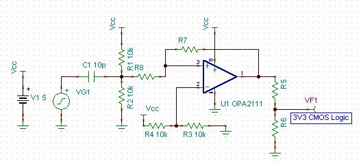
The circuit below is just for reference, as the values are not defined.

Input signal Vg is a 100 kHz to 300 kHz  (almost) square wave with 700 mV amplitude.

R1 and R2 bias the AC coupled input to mid 5V rail.

R4 and R3 set the comp reference to mid 5V rail.

R8 and R7 add a little bit of hysteresis to the comparator.

R5 and R6 form a voltage divider to interface to 3V3 logic ( microcontroller)

What parameters should I analyze to evaluate the behavior of this circuit?

There is any recommendation on additional circuit to be added to improve its behavior?

Thank you all and kind regards,

Alexandre Martins

  • Alexander,

    You mentioned OPA211 in the title of your forum post but your schematic shows OPA2111 - these are two completely different op amps; bipolar vs JFET, respectively.  Are you attempting to use OPA2111 or OPA211?  If former is the case, the minimum supply voltage for OPA2111 is +/-5V (10V total) and you attempt to use it with +5V single supply thus violating min Vsupply PDS specification.  If latter is the case, you may NOT use OPA211 as a comparator because it uses back-to-back input protection diodes and thus input differential voltage must be limited to few hundred mV – see below.

  •  

    Hello Alexandre,

    Noting Marek's point about the OPA211 and OPA2111, I am going to assume you intend to use the OPA211 because that amplifier is listed in the title and text.

    Like most operational amplifiers, the OPA211 can be applied as a comparator. But because it has back-to-back diodes across the inputs as shown in data sheet Figure 45, and its common-mode voltage input range (Vcm) does not extend to the power supply rails, precautions should be taken to assure it is not overdriven. The OPA211 is specified with a Vcm of minimum of (V-) + 1.8 V, and maximum of (V+) - 1.4 V. Therefore, the CMV range is +1.8 V to +3.2 V, with a +5 V supply.

    I set your circuit up in our TINA-TI Spice simulator to see what the input levels look like heading into the OPA211. You can see the TINA circuit below. The input signal was set to a square wave having an input frequency of 300 kHz and amplitude of 700 mVp-p. The amplitude was kept to this level to keep the back-to-back input diodes turned off. I set up the hysteresis resistors, R3 and R6 in my diagram, for about 50 mV of hysteresis.

    The waveforms located directly below the comparator schematic show the generator input signal (light green), the signal at the OPA211 non-inverting input (brown), and at signal at the comparator output (dark green). The generator input is a square wave as expected, but the signal seen at the comparator input has been differentiated resulting in voltage peaks associated with the square wave edges. The output appears similar to a square wave, but that is probably because the OPA211 output is being driven from one supply rail, to the other. There is overload recovery time associated with coming out of output overload. The output spends some time at each supply rail level.

    The waveforms on the upper right are with the 10 pF input capacitor changed to 10 nF. This was to observe how the OPA211 output changed when the square wave wasn't being passed through a differentiator circuit before entering the amplifier input. The output appears to be more decisive at the start of the waveform, but otherwise similar to what was seen in the first waveform diagram.

    Since there is concern about not exceeding the OPA211 Vcm range and/or turning on the input clamp diodes, a 5 kΩ series resistor was added between the signal generator and the inverting input. Note that this resistor was not in the circuit when the previous two waveform sets were taken. The 5 kΩ resistor sets up a 0.5 V/V voltage divider with R4 and R5, and the input voltage is reduced from about 700 mV, to 350 mV. You may want to consider adding a series input resistor to limit the input voltage swing.

    Regards, Thomas

    PA - Linear Applications Engineering

  • All,
    Depending on the size of the input cap, C1, the peak Vin voltage at the inverting input terminal may increase, potentially leading to forward biasing of one of the back-to-back input protection diodes-that will be especially true at the elevated temperature when the voltage required to turn-on the diode decrease down to between 200mV and 300mV. This condition will lead to the current flowing thru one of the input diode resulting in voltage drop across R3 resistor thus causing shift in a tripping point voltage. For more info, please read the blog covering this topic:

    e2e.ti.com/.../op-amps-used-as-comparators-is-it-okay
  • Hi,
    Thank you all for the replies.
    I am trying to use a OPA211. I am sorry for the mistake in the schematic.
    In fact, I am using OPA211SKGD1, for use in a high temperature application (reaching 200 ºC).
    The amplifier was selected for signal conditioning and I was trying to reuse the part.
    The input signal comes from a series resonant tank at 100kHz to 300 kHz, whose voltage can reach about 60-100 V peak.
    I need to measure the frequency of this signal. I was thinking of clipping this voltage with two diodes to ground, thus resulting in a -700 mV +700 mV signal. Then convert the signal to digital.
    With such temperature rise the turn-on voltage of the input diodes of the OPA211 will surely decrease.
    Maybe trying a different approach and try to feed the signal to a ADC of the DSC (a SM320F28335-HT)?

    Thank you.
    Best regards,
    Alexandre Martins