This thread has been locked.

If you have a related question, please click the "Ask a related question" button in the top right corner. The newly created question will be automatically linked to this question.

OPA2227 as reference buffer for ADC. Instability problem.

Other Parts Discussed in Thread: OPA2227, ADS7229, OPA227, TINA-TI

Dear TI Support,

I am writing you regarding the circuit which consists of 16 independent acquisition channels each one having an Input multiplexer, a conditioning stage (OPAMPs) and an ADC (ADS7229) . The reference is generated by the MAX6175AASA+ and the OPA2227 configured as voltage follower is used to buffer the reference to the 16 ADCs.

Every ADC reference pin is decoupled with a 22uF capacitor as described in the ADS7229 datasheet. My plan was to use the same buffer output to buffer all the ADC or to use maximum two different OPA2227 to decrease the capacitive loading.

The question I have is about the sub-system Reference – ADCs:


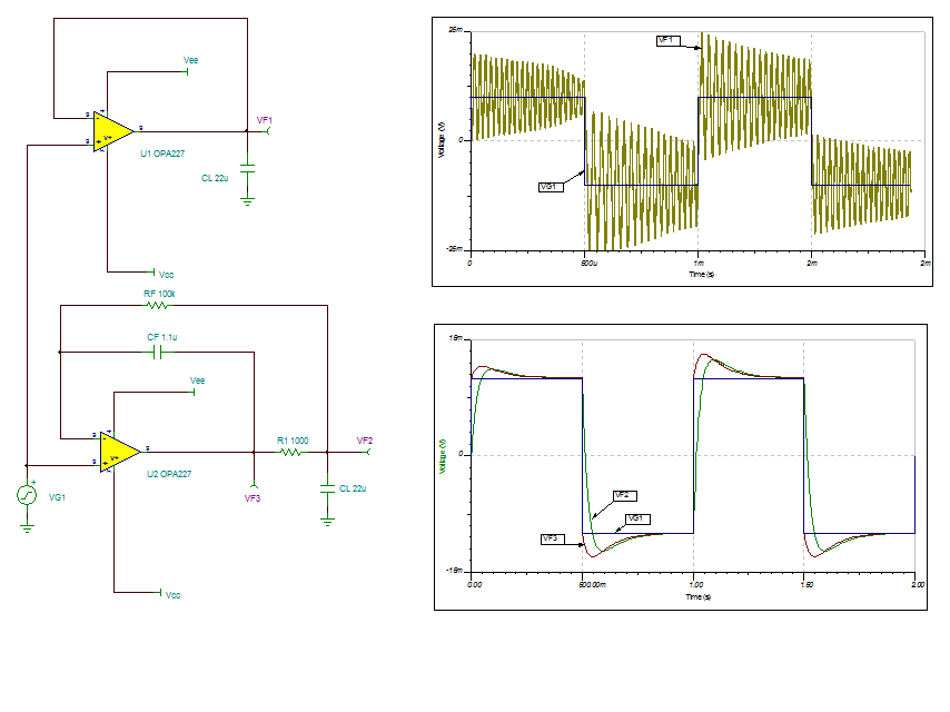
After noticing oscillations on my prototype, I added the capacitor C9 and Resistor R11 on the voltage follower feedback loop in order to get a good phase margin and avoid instability due to the additional pole introduced by the load capacitors. I am currently trying to find the right values for those components. For doing this, I am using TINA TI in order to simulate the opamp circuit. Please find attached the TINA project where I simulate the effect of the total load capacitance of (22uF+100nF)x8=176uF+800nF and total load resistance ≈5kOhm.

-          The first thing I notice is that in the Transient simulation I don’t see any oscillation (except from the initial ringing)

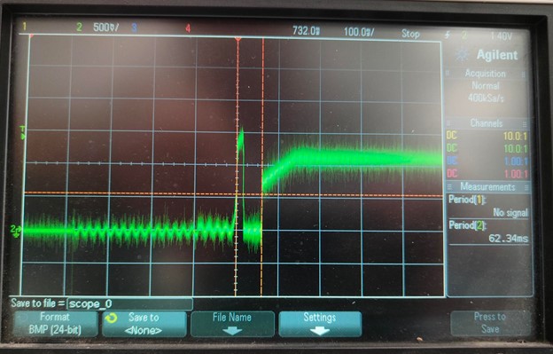
-          If I export the spice model of the OPA227 into another commercial simulator I can clearly see the instability in the time domain

-           I made the AC test circuit to simulate the AolB transfer function. The result I get with the chosen components values is 180degrees of phase before the 0dB, therefore the circuit should be instable. However, as I mentioned, in the time domain I don’t see any oscillation.

Could you please tell me if I am doing something wrong in the simulation or/any advice?

Thank you very much in advance.

Regards,

OPA2227_AC.TSC

  • Matteo,

    The OPA2227 macro-model available on TI website is the original, seventeen years old, version and it does not properly model circuit stability.  I have attached in this post new much more sophisticated version - please use it for your simulations.

    Also, in your double-loop configuration used to improve the capacitive load drive of OPA2227, you need to add a feedback resistor, RF, to poperly stabilize the circuit - see below.  

    The rule of thumb is to design the circuit for VF3 small-signal overshoot of 25% or less (>40 degrees phase margin) with absolute maximum allowable overshoot of 50% or less, which correlates to a minimum phase margin of 25 degees - see table below.

    Below please find the Tina-TI circuit schematic and the presentation covering the topic of circuit stability including details how to choose the component values for double-loop configuration - see page 61.  I also encourage you to watch the series of  TI Precision Labs  videos addressing in greater detail the issue of circuit stability:  

    OPA227 Reference buffer.TSC

    Op Amp Stability.pptx

  • Dear Marek,

    thank you very much for your complete and clear answer.

    Regards,

  • Hello,

    I have finally developed the final version of the board. This consists on a single reference chip (MAX6185), the OPA2227 used to buffer the reference. The output of the buffer goes to the 16 reference pins of the ADCs (ADS7229). Every ADC reference pin has a 22.1uF capacitor next to it. The opamp has been compensated to capacitive loads following the post.

    Unfortunately, I see the following:

    - the OPA2227 heats up to 47degrees

    - If I look with an oscilloscope at the output of the buffer I dont see oscillations until the ADC input value (VIN_ADC) reaches +10V (for +11V there is no oscillation)

    - If I slightly vary the input voltage (example: from 9.999 to 10) the oscillation does not occurs

    - If I touch the compensation network the oscillation stops and appears again if I vary the voltage to +10V

    - The oscillation appears only when the ADCs are converting. If I stop the conversion, the oscillation does not occur in any case. 

    - If I let only 2 ADCs convert, the oscillation does not occur.

    Since there is no oscillation when the ADC are not converting, I assumed that the OPAMP was properly compensated. I also tried to decrease the capacitive load from (22.1uF x 16) to (10.1uF x 16) and the behaviour was exactly the same. Therefore I would say that the oscillation is caused by the sampling of the ADC which introduces additional stress into the OPAMP.Additionally, what I cannot explain is why this happens only to a specific input value. 

    Thank you in advance for any help,

    matteo