This thread has been locked.

If you have a related question, please click the "Ask a related question" button in the top right corner. The newly created question will be automatically linked to this question.

LOG114 unexpected output behaviour

Other Parts Discussed in Thread: LOG114

Hi,

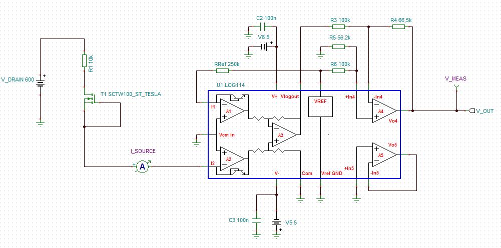
I am trying to use LOG114 to measure a small quiescent current of a power MOS. I started working using the datasheet dual-supply configuration and the simulations gave quite good results using a reference current (I1) of 10uA (VREF = 2.5V RRef = 250K).

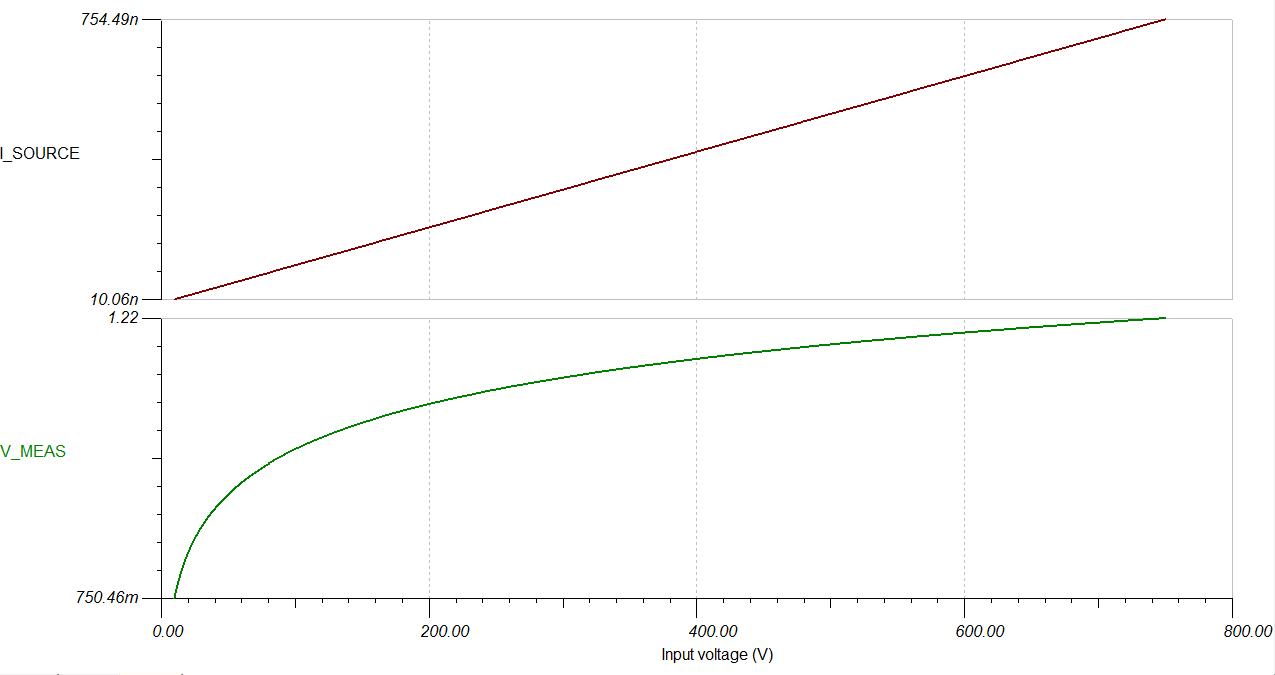
After this I tried to build a small circuit to evaluate its "real" behaviour and I found out for current values above 2uA everything works fine but for current values lower than 2uA I get negative, "fluctuating" VOUT values:

  • I = 0,4uA - VOUT = -0,581V
  • I = 0,5uA - VOUT = -0,484V
  • I = 1uA - VOUT = -0,250V
  • I = 2uA - VOUT = 1,240V
  • I = 5uA - VOUT = 1,413V
  • I = 10uA - VOUT = 1,488V

I guess there is something to be tuned on A4 Op Amp input/feedback resistances. How can I improve the circuit to get positive stable output values on the whole range (10nA - 1mA)?  

Thanks,

Enrico 

  • Hello Enrico,

    Conceptually, I don't find anything incorrect about the way you are applying the LOG114 in the circuit.  Do keep in mind that as the input current is reduced to very low levels the log amp transimpedance gain becomes very high. When it operates with very high gain the circuit becomes more susceptible to stray circuit currents and reacts more readily to fields present where the PC board is located.

    You mention the output voltage is fluctuating. I have seen this occur when the LOG114 is receiving 50/60 Hz fields generated by the ac power lines present in the lab. The fluctuating output is evident with an oscilloscope attached to the amplifier circuit output. 

    You didn't mention your circuit construction methods but the LOG114 must use PC board construction. Likely, the board will need to be mounted inside a closed metal enclosure. This will help reduce the ac fields being induced into the LOG114 PC board. The supply lines in and out of the metal box need to be properly bypassed and any signal lines in, or out, of the box should use shielded cables and connectors. Also, the PC board should be ultrasonically cleaned after any soldering operations to minimize stray leakage currents associated with residual flux contamination.

    The LOG114 is capable of amplifying very low currents and meeting the accuracy specifications in the datasheet. However, that can only be achieved when it is operated in the properly established circuit environment. If you haven't seen the LOG114 EVM information already, you may want to do so for additional information about applying the device.

    Regards, Thomas

    PA - Linear Applications Engineering

  • Hi Thomas,
    first of all thank you for your fast reply! I will definitely use your advices to design the final PC board!

    In order to repidly validate this solution in the Lab I actually used a "wired" board and a VQFN socket. So I understand this may not be the best solution in terms of noise/EMC and small current measurements.

    What made me suspect there is something wrong in the design is this kind of "jump" between 1uA and 2uA. Changing the I_Input of just 1uA I found something like 1V output difference (from -0,250V to 1,240V). And moreover the "negative" output is something I did not excpect.....could even this be related to the "wired solution"?

    Thank you very much for your support!

    Enrico

    PS I will receive a small PCB prototype on Friday afteroon. I will be able to give you a more exhaustive feedback in a while.....

    Thank you.

  • Hi Enrico,

    The LOG114 has a power pad that is intended to be soldered to a copper pad on the PC board that is connected to the V- supply. If this pad is not soldered and connected as intended the behavior of the LOG114 may not be good. Did you connect the pad as directed in the datasheet in your prototype assembly? If not, you may find that you may not be able to achieve correct electrical performance until you do so. 

    Regards, Thomas

    PA - Linear Applications Engineering

  • Hi Thomas,

    yes, the socket we used has a central pin-pad that allow the connection of VQFN IC's central pad. We connected it to V- as mentioned in the datasheet.....

    I really hope it is a "soldering-wiring-prototype" issue and the PC board we are going to receive will solve this issue....

    Regards,

    Enrico

  • Hi Enrico,

    The LOG114 is a solid performer when it is applied in a well designed electrical and thermal environment. My experience has been that when a user has had difficulties obtaining the expected performance the source of the issue has been traced to board layout, board cleanliness, inadequate shielding from fields, etc. and not the device. 

    You may want to take a look at the LOG114 EVM board for some ideas about the PC board layout:

    Regards, Thomas

    PA - Linear Applications Engineering